This thread has been locked.

If you have a related question, please click the "Ask a related question" button in the top right corner. The newly created question will be automatically linked to this question.

DS90UB960-Q1: Is Waveform generated by UB960 patten generation normal?

Part Number: DS90UB960-Q1

We are using PatGen mode of ds90ub960 to generate (1280*720, RAW8) fake data to CSI-2 port 0 and  NVIDIA Orin was used to read the CSI-2 data.

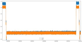
We have probed the CSI0_D3P and CSI0_D3N pins but both the voltage level range and waveform are odd.

Figures below shows the waveform from Oscilloscope:

Question:

1) We noticed the signal voltage level is range from 0-500mV during HS transmit. That is not the typical value(200mV) and even over the MAX(250mV) range which recommended in the MIPI D-PHY handbook. Will the output voltage can be a problem for Orin to read the data? 

2) The voltage level of the signal in HS mode is not fixed, which is changed from 150mV to 500mv(From the figure, it includes several completely different waveforms in HS mode). Is it normal?  If normal, does each segment of the waveform represent a different meaning?

  • Hi Guo,

    Can you provide more details about the test setup and how you are measuring these signals (type of oscilloscope, probe, etc.)?

    Regards,

    Cindy

  • Thanks for your reply, the details are given below:

    - Test Setup:
    (Refer to 'Analog LaunchPAD v1.57.0010\PreDefScripts\DS90UB954\954_CSI_patgen_RAW8_1920x1080p30.py' )
    ```
    board.WriteReg(0x33, 0x03)

    board.WriteReg(0xB0, 0x02) # IA_AUTO_INC=1
    board.WriteReg(0xB1, 0x01) # PGEN_CTL

    board.WriteReg(0xB2, 0x01) # PGEN_ENABLE=1
    board.WriteReg(0xB2, 0x33) # PGEN_CFG
    board.WriteReg(0xB2, 0x2A) # PGEN_CSI_DI
    board.WriteReg(0xB2, 0x07) # PGEN_LINE_SIZE1
    board.WriteReg(0xB2, 0x80) # PGEN_LINE_SIZE0
    board.WriteReg(0xB2, 0x00) # PGEN_BAR_SIZE1
    board.WriteReg(0xB2, 0xF0) # PGEN_BAR_SIZE0
    board.WriteReg(0xB2, 0x04) # PGEN_ACT_LPF1
    board.WriteReg(0xB2, 0x38) # PGEN_ACT_LPF0
    board.WriteReg(0xB2, 0x04) # PGEN_TOT_LPF1
    board.WriteReg(0xB2, 0x65) # PGEN_TOT_LPF0
    board.WriteReg(0xB2, 0x0B) # PGEN_LINE_PD1
    board.WriteReg(0xB2, 0x93) # PGEN_LINE_PD0
    board.WriteReg(0xB2, 0x0A) # PGEN_VBP
    board.WriteReg(0xB2, 0x0A) # PGEN_VFP
    board.WriteReg(0xB2, 0xAA) # PGEN_COLOR0
    board.WriteReg(0xB2, 0x33) # PGEN_COLOR1
    board.WriteReg(0xB2, 0xF0) # PGEN_COLOR2
    board.WriteReg(0xB2, 0x7F) # PGEN_COLOR3
    board.WriteReg(0xB2, 0x55) # PGEN_COLOR4
    board.WriteReg(0xB2, 0xCC) # PGEN_COLOR5
    board.WriteReg(0xB2, 0x0F) # PGEN_COLOR6
    board.WriteReg(0xB2, 0x80) # PGEN_COLOR7
    board.WriteReg(0xB2, 0x00) # PGEN_COLOR8
    board.WriteReg(0xB2, 0x00) # PGEN_COLOR9
    board.WriteReg(0xB2, 0x00) # PGEN_COLOR10
    board.WriteReg(0xB2, 0x00) # PGEN_COLOR11
    board.WriteReg(0xB2, 0x00) # PGEN_COLOR12
    board.WriteReg(0xB2, 0x00) # PGEN_COLOR13
    board.WriteReg(0xB2, 0x00) # PGEN_COLOR14
    board.WriteReg(0xB2, 0x00) # Reserved
    ```

    - Measuring:
    Oscilloscope: Keysight DSV334A Oscilloscope
    Probe: Keysight N5449A adapter + N2873A probe(10:1)
    Figure: Y-axis voltage / v, X-axis time / s
    Probed pin: D3N: blue line, D3P: orange line

  • Hi Guo,

    The data lanes need to be connected to a termination in order to properly measure the HS burst sequence. Are the pins connected to the NVIDIA Orin or a termination board? 

    Regards,

    Cindy

  • Yes, the pins are connected to the NVIDIA Orin.

  • Hi Guo,

    Can you check that the NVIDIA Orin is configured to D-PHY mode and not C-PHY mode

    If this is true, can you try measuring the pins directly on a scope instead, making sure there is a 100Ohm termination across the pins?

    Regards,

    Cindy

  • Hi Cindy,

    I'm Guo's colleague.

    Our Orin uses D-PHY mode.

    For the waveform above, we are wondering if it is reasonable that the signal seems to have different high and low levels in different areas?

    Thanks a lot,

    Lee

  • Hi Lee,

    The measurement does not look as expected. The high speed burst between the LP states should not have such varying voltage swing, and the voltage should also not exceed the MIPI specification. I would try measuring this directly on a scope with a termination or check the test setup/connections.

    Regards,

    Cindy

  • Hi Cindy,

    We shall appreciate hearing the results from you.

    Besides, I would also like to know if certain configurations in Jeston Orin will change the wavefrom of the CSI-2 data lane ?

    Best,

    Lee

  • Hi Lee,

    Sorry for confusion, I meant that your team should try to measure directly on a scope to see if you still get the same waveform. All of our MIPI CSI-2 parts including the 960 have been validated to pass the MIPI specifications, so the results you are seeing may be due to an issue with the test or measurement setup. For your last question, it would be best to contact NVIDIA directly to see if they can help you with the Orin configs.

    Regards,

    Cindy 

  • Hi Cindy,

    Sorry for the late response,

    1. We checked the output signal again, the data lane waveform still looks the same. But in the clock lane, a voltage of 0.5V lasts for about 50ns, occurred at LP11-LP01-LP00 switching both in CLKN and CLKP. Also, the clock does not seem to toggle during HS. We are all confused about this problem.

    2. As the configurations in the PatGen script, the output frame has been set to 1280*720 30FPS and the data rate is 400Mbps. As MIPI CSI2 specification, each faram should contain 720 long packets and each packet should send 1280byte. So to sepak, the time taken to transmit each long packet per lane should be approximately ((32bit(header) + 1280*8bit + 16bit(footer)) * UI) / 4lane = 6430ns. But our long packet transmission only takes about 4200ns.

    Could you please give me some ideas on the problems I mentioned above?

    Thank you very much,

    Lee

  • Hello Jim,

    Cindy is Out of office and will be back in 3 days.

  • Hi Hamzeh,

    Thank you for your information.

    I post the waveform below for the first point in my last reply:

  • Jim, Thanks for your patience

  • Hi Jim,

    1. Can you try running the CSI transmitter in continuous clock mode (Reg 0x33) and measure the waveforms again? 
    2. Can you share what your 960 patgen register configurations are so I can double check the timing?
    3. The line time speed depends on the REFCLK as well. Are you using 25MHz? Also note that the line period in patgen registers 0x0C-0x0D has different units for 400Mbps (20ns units), so this should be taken into account when you are programming. 
    4. Also since you are running at 400Mbps, have you programmed the necessary additional registers as outlined in section 7.4.19 in the 960 datasheet?

    Regards,

    Cindy

  • Hi Cindy,

    Thank you for your reply.

    1. We had tried to use the continuous clock mode, in this case we can not get any output from the UB960, which could also be a strange thing.

    2. We simply use the pagtern generator code example in the UB960 manual section 7.5.12.4 for 400MHz, and the configuration for 800MHz is the same as the one mentioned above.

    3. It is 25MHz, we had confirmed this configuration with the help of an oscilloscope. Could you share me more information about the relation with 400Mbps and 20ns units?

    4. Yes, we noticed the additional is required in UB960 handbook and programmed them.

    Best,

    Lee

  • Hi Jim,

    1. If you are using the SOC, no output can mean that the SOC does not support this clocking mode. Continuous clock means that the signal remains in HS mode, so it is possible that there are termination issues on the receiving end. 
    2. Is the SOC reporting any errors in receiving the data?
    3. Are you able to try patgen on another 960 board or a 960 EVM to see if you see the same waveform on the data lanes?
    3. It is 25MHz, we had confirmed this configuration with the help of an oscilloscope. Could you share me more information about the relation with 400Mbps and 20ns units?

    At 400Mbps, the units for the line period patgen register is 20ns, so this is the unit used to convert from the line period to the register values in 0x0C-0x0D. If you left it as default then the video line period is 63.5us. 

    Also, the clock does not seem to toggle during HS.

    Have you been able to double check whether the Orin/receiver settings are configured correctly as well? For the transition into HS mode, there must be a proper D-PHY termination otherwise the quality of the signal is affected. 

    Regards,

    Cindy

  • Hi Cindy, 

    Thank you for your kind words!

    1.

    SOC reporting any errors in receiving the data

    We read the video stream from V4L2 and the errors were caused by D-PHY. We decode the error status code with the tool "nvcapture-status-decoder", the output is shown below:

    NVIDIA camera capture status decoder utility (Version 2.00)
    Copyright (C) 2019-2020, NVIDIA Corporation. All rights reserved.
    
    Class: Global
    Type: PHY_Interrupt0
    PHY: 0
    CIL: 0
    Stream: 0
    VC: 0
    Status: 136
    Timestamp: 2470133328
    
    PHY_Interrupt0 : 0x0000000000000088
        -cil_data_lane_ctrl_err0     [ 3]: 1
            LP sequence error detected on data lane [A/B]0
    
        -cil_data_lane_ctrl_err1     [ 7]: 1
            LP sequence error detected on data lane [A/B]1
    
    Class: Global
    Type: PHY_Interrupt0
    PHY: 0
    CIL: 0
    Stream: 0
    VC: 0
    Status: 128
    Timestamp: 2470133328
    
    PHY_Interrupt0 : 0x0000000000000080
        -cil_data_lane_ctrl_err1     [ 7]: 1
            LP sequence error detected on data lane [A/B]1

    In addition, the 0x00000088 error was only prompted twice at first, and the 0x00000080 error was prompted constantly.

    2.

    Orin/receiver settings are configured correctly as well?

    Could you please explain in more detail what the settings are indicating?

    3.

    We have another UV960 board and had already tried, the output is in the same.

    Best,

    Lee

  • Hi Lee,

    Thank you for the additional information.

    Could you please explain in more detail what the settings are indicating?

    This would include making sure the receiver CSI-2 settings are configured to match what you programmed in the deserializer (number of data lanes, data rate, continuous or non-continuous clock). I would contact NVIDIA directly about configuring this if you have more questions. 

    Are you using a custom designed UB960 board? If so, you may want to double check it is not a layout issue with the CSI-2 traces (TI can help you review this if you submit another E2E requesting it). You can try testing with a 960 EVM if you have one to rule out a layout issue.

    I suggest reaching out to NVIDIA about the LP sequence errors. Given that 1) the other 960 board is causing this error as well and 2) you are configuring patgen + CSI-2 forwarding following the Patgen section of the datasheet, it may be software related on the receiving side since your SERDES config is all correct. You can send your full 960 script to me if you want me to double check your CSI-2 settings since the last one you sent does not include the speed configuration.

    Regards,

    Cindy