Part Number: DP83TG720S-Q1
hi team,
customer had some problems debugging the DP83TG720S-Q1 PHY chip.
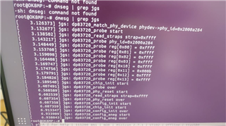
When reading the PHY chip's register via MDIO, the returned value received is incorrect.
the follow information is customer's configure and test result.
The PHY is configured as follows
The PHY is in Master mode
Interface RGMII alignment mode
The address of the PHY is 0x00 0 C 12
Also configure AUTO to be autonomous
problems found during debugging and how to handle them
The MDIO pins were designed without pull-resistance and were pulled up to 3 .3V by flying lead 2 .2K
The WAKE pin software does not have hardware configured and is pulled directly to 3.3V by flying lead
Also use the R X_CTL pin and S TRP_1 according to the chip manual RX_CTL configuration resistance not soldered when configured P HY address 0x 000C 1 2 Soldered 1 3K pulled up to 3 .3V
you can also see the schematic and lay out in the attached file.Copy of DP83TG720_Schematic 0523.xlsxAnnex2-5gxx-230423b.pdf
The values of the read data registers 2 and 3 via MDIO are P HYID0 x FFFF, occasionally reading the correct value