This thread has been locked.

If you have a related question, please click the "Ask a related question" button in the top right corner. The newly created question will be automatically linked to this question.

SN65DSI83: LVDS screen corrupted when using the DSI83

Part Number: SN65DSI83

Hello everyone,


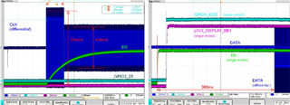
We are working on a custom i.MX8M-mini Android 11 based device which uses the SN65DSI83 MIPI DSI to LVDS bridge.

In general terms, our device works correctly, however we have noted a very sporadic issue, we need to turn on/off our device screen several times for it to occur. As you can see o the attached f1.png image, when the issue happens the upper half of the screen is corrupted, meanwhile the lower half of the screen remains working correctly.

TI-images.zip

This issue is normally fixed by locking and unlocking our device screen for the LCD to be reinitialized, but we need to understand the corresponding root cause.

We have tried many display timings on our Linux LCD drivers according to the display datasheet and setting additional delays on the DSI83 driver without success.

We noted that when the issue occurs, if we send a test pattern from the DSI83 (0x3C = 0x10) the glitch is not visible, but when returning to normal video stream (0x3C = 0x00) the screen issue is there again, this make us think that the issue is on the MIPI DSI portion of our i.MX CPU, but we reached you out to see if you could provide us any debugging step from the DSI83 perspective.


Any suggestion will be highly appreciated,

Thanks, and best regards,

Esteban V.

  • Esteban V

    When you are turn on/off the device screen, are you doing power cycling to the MIPI SOC or DSI83? 

    If you clear the register 0xE5 by writing 0xFF, and then read the register again when this particular issues happens, are you seeing any bit in register 0xE5 being set? 

    If you set the SOFT_RESET bit when this issue happens, does that also fix the issue?

    Thanks

    David

  • Hello David,


    Thank you for your quick response, regarding your questions, please find my comments below.


    1.- When turning off our device screen Linux/Android powers off the MIPI DSI portion and from the DSI83 perspective, the OS sets low the EN signal, then clears reset (0x9 register) and disables the PLL (0xD register).


    2.- We are using a slightly different version of the following driver.

    https://elixir.bootlin.com/linux/latest/source/drivers/gpu/drm/bridge/ti-sn65dsi83.c#L487

    Currently I commented out lines 488 & 489 which clear the errors after the initialization.

    I reproduced the issue two times, the first I read 0xE5=0x89 and the second one I read 0xE5=0x49, but as can be seen below, when manually clearing the error register, non-errors were persisted.

    #First time.
    
    ams_trex_8mm:/ # i2cget -y -f 0x3 0x2d 0xe5
    
    0x89
    
    ams_trex_8mm:/ # i2cset -y -f 0x3 0x2d 0xe5 0xFF b
    
    ams_trex_8mm:/ # i2cget -y -f 0x3 0x2d 0xe5
    
    0x00
    
    #Second time.
    
    ams_trex_8mm:/ # i2cget -y -f 0x3 0x2d 0xe5
    
    0x49
    
    ams_trex_8mm:/ # i2cset -y -f 0x3 0x2d 0xe5 0xFF b
    
    ams_trex_8mm:/ # i2cget -y -f 0x3 0x2d 0xe5
    
    0x00
     

    3.- If I set the SOFT RESET on runtime, using the command below, the screen flickers a little bit, then returns normal operation, however when the issue occurs, the visual inconsistencies are there before and after executing the commands.


    ams_trex_8mm:/ # i2cget -y -f 0x3 0x2d 0x9
    
    0x00
    
    ams_trex_8mm:/ # i2cset -y -f 0x3 0x2d 0x9 0x1 b


    Looking forward to your comments,

    Thanks, and best regards,

    Esteban V.

  • Hi Esteban,

    Are you following the initialization sequence in Table 7-2 of the datasheet? Can you use a scope to ensure the CLK is in HS state and data is in LP11 state when EN pin goes from low to high?

    Thanks, Allison

  • Hello Allison,


    Sorry for the late response, we are reviewing your recommendations regarding the measurements, the code seems to follow the correct sequence, but we need to double check the signals on the scope, as our i.MX8 device is a tablet with a case, it’s quite difficult to measure the requested signals but we are working on it.


    We will keep you posted with our findings,

    Best regards,

    Esteban V.

  • Hello Allison and David,


    We obtained the requested measurements, please find below a description of each one of the attached images.

    1.- NOKStart.bmp: Shows the CLK, data and EN signals when the EN pin goes from low to high, in this case the LCD corruption issue was observed.

    2.- NOK01.bmp: Shows the CLK, data and EN signals during the video transmission, in this case the LCD corruption issue was observed.

    3.- OKStart.bmp: Shows the CLK, data and EN signals when the EN pin goes from low to high, in this case the LCD corruption issue was not observed.

    4.- OK01.bmp: Shows the CLK, data and EN signals during the video transmission, in this case the LCD corruption issue was not observed.

     InitSequence.zip

    Could you please let us know if the involved signals behave as expected regarding the initialization sequence?

    Looking forward to your comments,

    Thanks, and best regards,

    Esteban V.

  • Hi Esteban,

    The DSI data lane should be in LP11 state before the EN pin toggles from low to high, as shown below:

    In your scope shots, the EN pin begins ramping before the data is in LP11 state. You can also add an external capacitor to the EN pin to delay the ramp.

    Best, Allison

  • Hello Allison,


    Thank you for your comments and inputs, it is important to say that currently our hardware controls the DSI83 EN signal through a capacitor as illustrated in the Figure 8 below.


    The measurements that we previously shared were done having a hardware rework for the EN signal to be controlled by a GPIO as illustrated on Figure 9.

    However, first we would like to understand if Figure 8 is a valid setup and what is the correct initialization sequence on this case because it cannot be delayed in case of a standby (i.e., locking and unlocking our tablet display) as it's always HIGH after power on.


    Looking forward to your comments,

    Thanks, and best regards,

    Esteban V.

  • Hi Esteban,

    Both configurations are valid setups, and they both need to follow the same initialization sequence that I provided previously.

    Does Vcc remain high during the locking/unlocking of the tablet display? If so, the DSI83 still needs to be reset, which can be done by following the same initialization sequence. When the DSI83 is reset while Vcc is high, the EN pin must be held low for at least 10 ms before being asserted high to ensure the device is properly reset. The DSI CLK lane must be in HS mode and the DSI data lanes must be driven to LP11 while the device is in reset, before the EN pin is asserted high.

    Best, Allison

  • Hello Allison,


    Thank you for your response. Regarding your questions, please find my comments below.

    1.- Yes, we measured VCC, and it is always high after powering on the device.

    2.- We are working on the corresponding initialization sequence, currently we are controlling the EN signal through a GPIO, please find the corresponding init-sequence illustrated below.


    As far as I saw on the previously shown measurement, the DSI clock and the DSI data signals are in LP11 for 2.28ms but then they went to HS, and this occurred before the EN signal went from low to high, is my understanding correct?


    Looking forward to your comments,

    Thanks, and best regards,

    Esteban V.

  • Hi Esteban,

    Thanks for your comments. Please see my responses below.

    1. Thanks for checking this. Again, please ensure you are resetting the DSI83 when the tablet is locked/unlocked.

    2. Are the clock and data lanes a single ended or differential measurement? If they are differential, HS mode peak to peak voltage is 140mV min, 200mV nominal, and 270mV max. If they are single ended, HS mode peak to peak voltage is 280mV min, 400mV nominal, and 540mV max. LP11 mode is just a constant high at 1.2V. Can you confirm if this is what you are reading? The DSI CLK must be in HS mode after power on, and the data lanes must stay in LP11 mode while EN pin ramps from low to high.

    Best, Allison

  • Hello Allison,


    Thank you for your response, we measure the requested signals, please find the results attached to this post.

    Approach 1 (12.07.2023).pdfApproach 3 (10.07.2023).pdf

    As per our understanding the clock is in HS long before the DSI83 EN pin is asserted, we are using a slightly different version of the following driver, in fact the approach#1 and approach#3 name on the PDF files refers to two different source code modifications that we tried for the EN signal to be asserted at the correct time.

    https://elixir.bootlin.com/linux/v5.15/source/drivers/gpu/drm/bridge/ti-sn65dsi83.c


    1.- Have you worked with the previously shown Kernel driver?

    2.- Have you implemented any workaround for this driver to achieve the expected power on sequence?

    3.- Does the power on sequence can affect the displayed image to cause the sporadic issue? (It is important to note that if we send a test pattern from the DSI83 the glitch is not visible but when returning the IC to normal operation the issue is there again).


    Looking forward to your comments,

    Thanks, and best regards,

    Esteban V:

  • Hi Esteban,

    We use I2C to initialize the DSI83, so we don't have specific DSI drivers. Is there a way you can try initializing the device using an I2C controller?  We cannot guarantee proper device function if the initialization sequence is not followed.

    With that being said, we do have an old reference code here: https://e2e.ti.com/support/interface/f/138/p/549283/2006135#2006135. It may implement an older version of the initialization sequence. You still need to follow the most up to date version of the initialization sequence that is in the datasheet. 

    Best, Allison

  • Hello Allison,


    Thank you for your comments and the reference code, when testing our latest software modifications, the power on sequence is determined by the measurements shown below.


    As far as I can see, the EN signal is being set high when the DSI CLK is in HS and the DSI data lanes in LP-11, I think that this covers the expected power on sequence, and the voltages seems to be within the expected ranges.

    However, the glitch still occurs (i.e., half of the image displayed on screen is sporadically corrupted) do you have any other suggestion for us to test from the SN65DSI83 perspective?


    Looking forward to your comments,

    Thanks, and best regards,

    Esteban V.

  • Hi Esteban, 

    With differential clock measurement, the peak to peak voltage requirement for HS mode is 140mV min, 200mV nominal, and 270mV max. Can you verify the clock reading on the scope is differential? The peak to peak voltage shown appears to be single ended. Also, the clock must be in HS mode for at least 10ms before EN pin begins ramping to high.

    Best, Allison