This thread has been locked.

If you have a related question, please click the "Ask a related question" button in the top right corner. The newly created question will be automatically linked to this question.

PCA9306: Back feed from SDA/SCL?

Part Number: PCA9306
Other Parts Discussed in Thread: TCA9509

Hi,

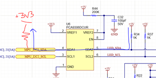
using the PCA9306 in a design and I would like to know if there can be a backfeed current issue through the SDA/SCL pins.

In this design, +5V rises first, and +3V3 follows a few milliseconds later. I understand there will be some leakage from VREF2 to VREF1, limited by the 200K. But what about leakage from the SDA and SCL signals? Can there be leakage current from SDA2 to SDA1, or from SCL2 to SCL2 from the 5V pull-up resistors?

Thank you

  • Hey Oliver,

    Yes there will be a leakage current flowing back into the lower side of the device during normal operation. The internal FET essentially acts as a strong resistor when a logic LOW is propagated through the device. This leakage current will flow from the 5V power supply, through the device and back into the 3.3V side. Note that the internal FET will be in an open connection when a logic HIGH is propagated, so side 1 is completely isolated from side 2, allowing the external pullup resistors to rise to their voltages. 

    If less power consumption is desired, the external pullup resistors need to be sized accordingly so that it is able to be achieved, (however there will be a speed trade off so your maximum achievable data rate will be limited).

    Here is an app note that goes in depth on how to calculate the values of the pullup resistors:

    Regards,

    Jack 

  • Hi Jack,

    thank you for your response. What I am concerned about is having current leaking between the 5V pull-up resistor and making the +3V3 rise before it should. As mentionned, 5V boots first and +3V3 boots later on. I'm trying to figure out if there can be a current flowing through the blue path below at power-up:

    thank you,

    Olivier

  • Hey Olivier,

    Thanks for clarifying your question. Your suspicion is correct as there will be a leakage from side 2 to side 1 when the 5V power supply is powered up first followed by 3.3V power supply. This is due to the EN pin shorted to the VREF2 power supply, so the device will be enabled at the time when the 5V power supply is ramped up. The voltage seen at side 1 will effectively be 0V since not powered on, further causing the FET to operate in the linear region where there will be a current passing through the FET.

    If this is of concern, is it possible to externally control the EN pin with an alt. power supply? (keep in mind that the voltage at the EN pin must be at least 0.7V above VREF1).

    Regards,

    Jack 

  • Hi Jack,

    thank you for the clarification. In this design I believe it will be an issue. I will change the translator for the TCA9509 instead.

    Thanks again,

    Olivier

  • Hey Olivier,

    Glad we are able to close that gap! Its important to note that with the TCA9509, pullup resistors are no longer needed on A side since there is an internal current source on that side. Please be sure that the VILC spec is able to be satisfied and the power supply recommendations mentioned in section 11 of the datasheet is taken into consideration. 

    Regards,

    Jack