This thread has been locked.

If you have a related question, please click the "Ask a related question" button in the top right corner. The newly created question will be automatically linked to this question.

DS90UB928Q-Q1: Insertion Losses due to Trace Length

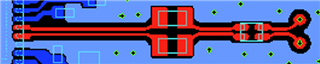
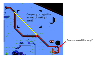
Part Number: DS90UB928Q-Q1

SI simulation engineer states that the only way to reduce insertion losses is to reduce the length trace from Connector to RIN+-, and use a different ESD Protection diode.
Currently we reduced from 80mm to 63mm but we still seeing the problem, could you recommend any other advice to improve?

  • Hi Jose,

    I will review and get back to you tomorrow.

    Regards,
    Fadi A.

  • Hey Jose,

    • I see your plot says S12 ... is this for a single ended trace? Our spec compares to SDD21 for an STP (differential pair)
    • What material are you using here?
    • Can you simulate the impedance for the entire high speed signal path?
    • What Pclk frequency are you using in this system?
    • Is this simulation done on the 928 PCB only or is including cable?

    A few things I noticed on the layout:

    What sized components are being used here for the CMCs? They look extremely large compared to the trace size which is probably causing impedance discontinuity (those pads will look very capacitive). If your differential impedance for those traces is lower than 100 ohms (+/- 10ohm) your insertion and return loss will be impacted significantly. 

    Can you get rid of sharp turns just go straight down to the connector and get rid of the connector loop.

    Another thing to note, if the 928 is on the top layer, the connector needs to be on the bottom later to avoid VIA stub. 

     Regards,

    Fadi A.

  • The Layout pictures @Katie Lee shared with your team are from the previous board, the new layout has been improved to shorthen the distance between the connectors to the CMC and IC. The connector is at the top layer due to customer requirement and it's true hole Molex connector HSAL-2.

    We run the SI simulations again don't populating the ESD diodes and the results are better on insertion/return losses:

    our application bandwidth is 1.05 Gbps / 526 MHz, do you see any risk if we are failing at the frequencies below?

    ØInsertion loss (SDD1,2) is fails at low frequencies before 350MHz and high frequencies after 1.54GHz

    ØInsertion loss (SDD1,2) fails in  0.03 dB difference at 1.8375 GHz

    ØInsertion loss (SDD1,2) passes in 0.03 dB margin at 0.527 GHz

  • Hey Jose,

    I will review and get back to you by end of today.

    Regards,
    Fadi A.

  • Hey Jose,

    Are you measuring the 928 PCB only or is this PCB and cable or is it the entire end of end system with both Ser/Des PCB plus cable? If cable is used here how long of a cable?

    Also, what's the different between green and blue graphs - are those differential measurements (SDD21) for each FPD port? Or are these single ended measurements for +/- of port0 only?

    All in all, The total transmission channel from SER to DES is the combined contribution from the SER‐board, cable assembly and the DES‐board. The PCB insertion loss budget, so higher insertion loss for the PCB is possible but with the trade‐off in lower insertion loss for the cable assembly. Our channel spec assumes 10 m cable plus a 2 inch trace, so if you are marginally failing on one side of the Ser or Des PCB as long as the total channel spec (2 PCBs + cable) meet the channel spec requirements provided in "Transmission Channel Requirement"  table in our spec then you should be ok.

    Regards,
    Fadi A.

  • Hello Fadi, I will reply back some of your questions above:

    Are you measuring the 928 PCB only or is this PCB and cable or is it the entire end of end system with both Ser/Des PCB plus cable? If cable is used here how long of a cable? Response: Only on PCB

    Also, what's the different between green and blue graphs - are those differential measurements (SDD21) for each FPD port? Or are these single ended measurements for +/- of port0 only? Response: Differential Measurements for each Port

    Response: 928 and Connectors are top side

    •  see your plot says S12 ... is this for a single ended trace? Our spec compares to SDD21 for an STP (differential pair)

    Response: it’s a differential

    • What material are you using here?, FR-4 4 Layers PCB, 
    • Can you simulate the impedance for the entire high speed signal path? The simulations includes the path from Connector to IC

    Response: Our intention is only PCB level

    • What Pclk frequency are you using in this system?

    Response: 30.13MHz

  • Hey Jose,

    For 30.13 Mhz PCLK you are in the passing range. 

    If you are trying to meet the spec for the overall frequency range, you still have additional margin in Cable budget which in our spec is defined for 10 m cable, plus another PCB for Deserializer, so the overall system budget is not as tight as a single PCB budget. As long as the overall budget meets the channel spec for "Transmission Channel Requirement" you should be ok. However, if the intent here is to pass the spec for the entire frequency range then the only solution with a 4 layer PCB I believe would be to make the FPD differential highspeed traces shorter. 

    Regards,
    Fadi A.

  • Hello Fadi,

    Thank you for your answers, that help us, unfortunately the layout doesn't allow us to make shorter the FPDLINK Differential traces...

  • Hi Jose,

    No problem, glad I can help. 

    Regards,
    Fadi A.