


Part Number: ISO1050
Other Parts Discussed in Thread: TPS62140A, , ISO1042
Hello Team,
we provide Vcc1 (+3.3V) and Vcc2 (+5V) power supplies to ISO1050 by means of two TPS62140A step-down converters, with Ratiometric and Simultaneous Start Up configuration (connected as described in SLVA470A).
The slopes of both output voltages are the same and the power supplies reach regulation in two different times, as shown in the following oscilloscope screenshot:
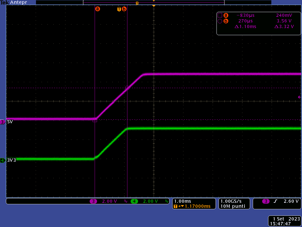
The soft-start time of 3.3V is about 1.1 ms. When Vcc1 reaches full regulation, Vcc2 = Vcc1 = 3.3V.
Vcc2 reaches full regulation (5V) about 1.7 ms after that EN is set.
My first question arises from the Table 8-1 at paragraph 8.3.3.3, where the device lockout and fail-safe conditions are shown:
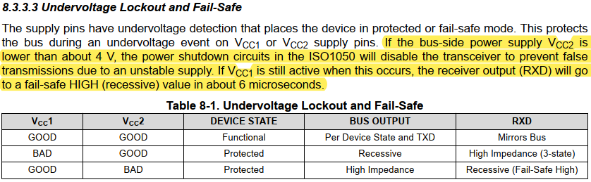
Is this above power-up sequence sufficient in order to guarantee that the bus output remains in High Impedance (no spurious commutations of the output) and
that the Receiver output RXD is in recessive state, until Vcc2 reaches full regulation?
According to ISO1050 datasheet SLLS983K paragraph 6.3, the minimum recommended operating condition for Vcc1 is 3.0V.
During start-up, when Vcc1 reaches the minimum recommended value (3V) also Vcc2 is at 3V (1V less than the 4V threshold specified at paragraph 8.3.3.3).
Provided that Vcc1 can be considered as GOOD above 3.0V, based on Table 8-1 I understand that
- with Vcc1 >= 3V and until Vcc2 reaches 4V, the transceiver is in lockout: the bus output is kept in High Impedance and the receiver ouput RXD is in recessive state (Fail-Safe High)
- after that Vcc2 has exceeded the threshold of 4V, the device enters normal operating conditions (typically in 300µs according to the datasheet at page 21)
Please note that we provide 4K7 pull-up resistors to Vcc1 on RXD and TDX lines.
A second question is related to the voltage threshold for Vcc2, which triggers the fail-safe mode of the device: what do you meand by "about 4V"?
Is there an hysteresis provided around this threshold? If so, how much in percentage?
Also, I noted that in previous datasheet Revision J (same paragraph 8.3.3.3) the undervoltage lockout threshold for Vcc2 was 2.7V instead of 4V. Why?
This change is not mentioned in the Revision History of the document. Is this due to a functional modification of the device or die change occured after September 2019?
Looking forward to hearing from you,
Thanks and Kind Regards
Lorenzo
