This thread has been locked.

If you have a related question, please click the "Ask a related question" button in the top right corner. The newly created question will be automatically linked to this question.

TCA9555: Interface forum

Part Number: TCA9555

Hi,

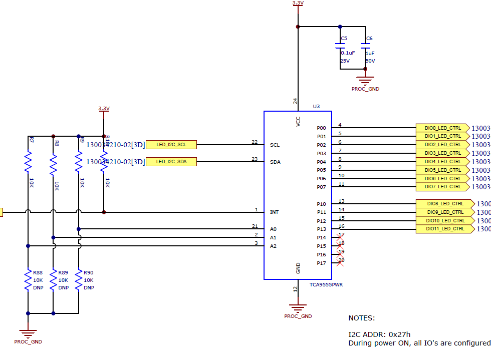
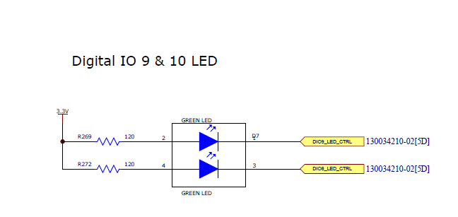
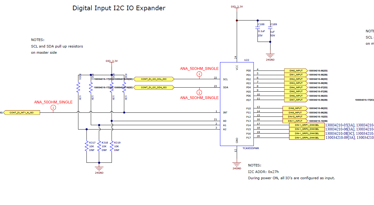
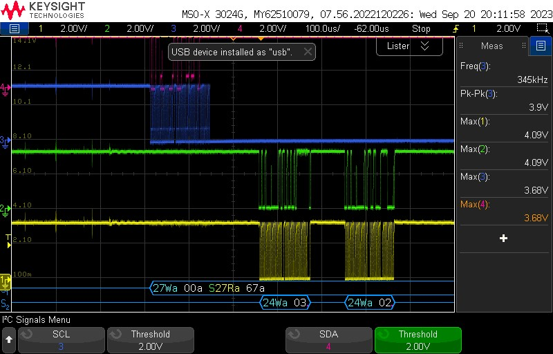
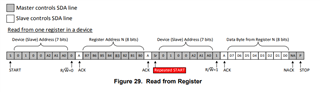
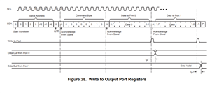
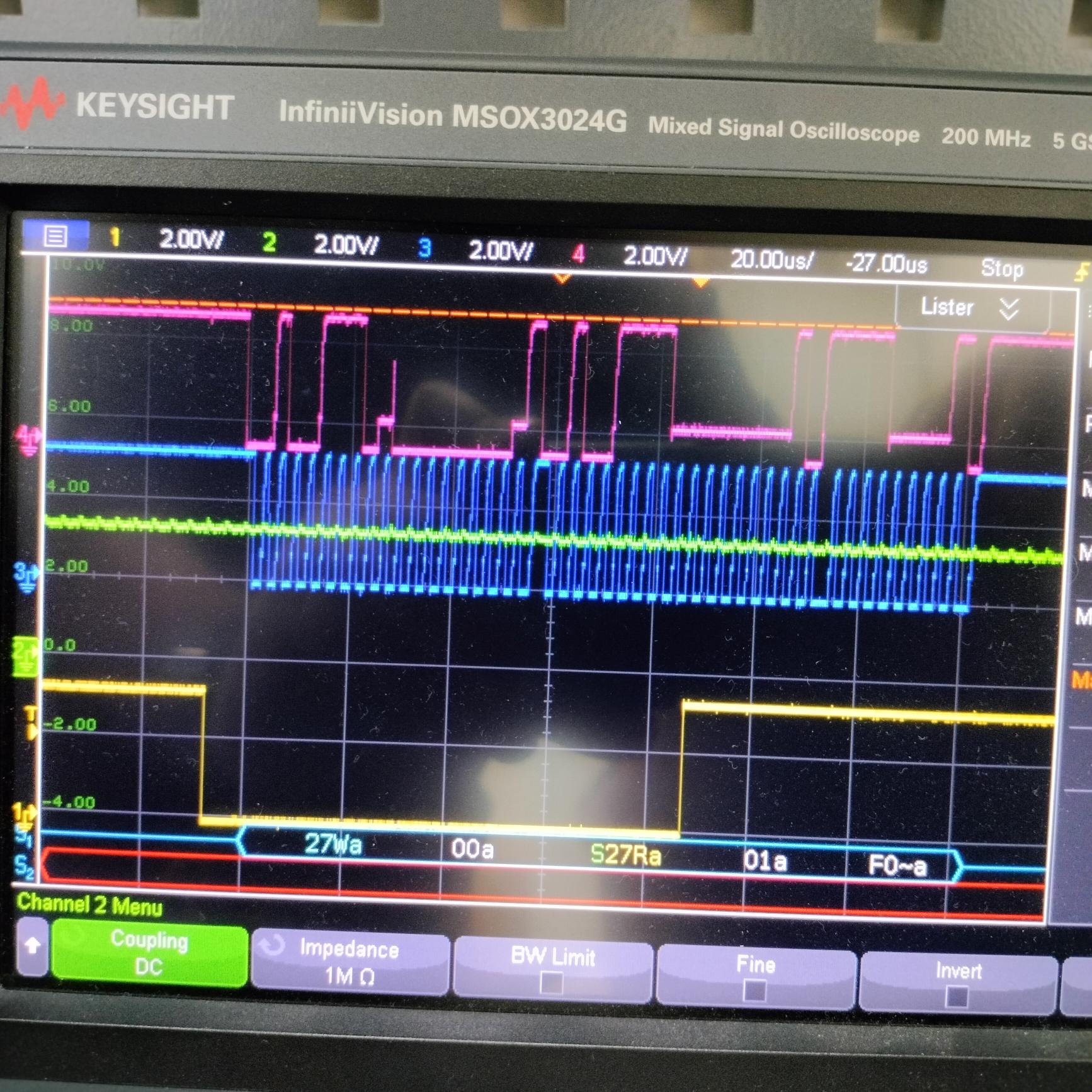
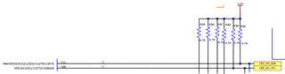
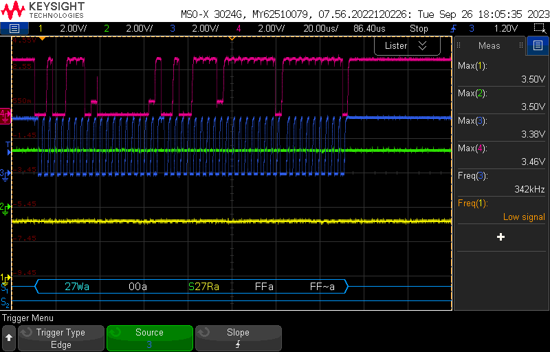
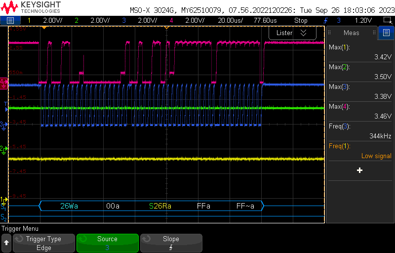
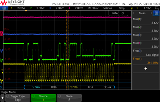
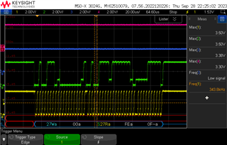
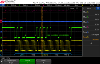
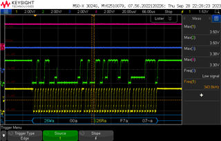
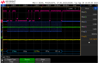
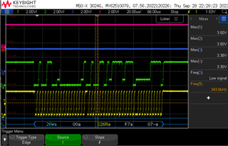
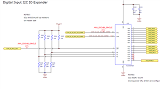
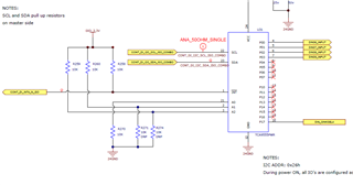
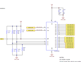
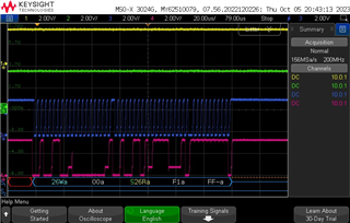
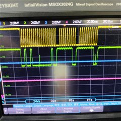
In my schematic, I've one set of IO expanders on which digital input will be applied and I'm reading the interrupt output of those IO expanders and based on those interrupts, another corresponding set of IO expanders are driven on which the LEDs are turned ON or OFF.

Please refer to my post :TM4C1294NCPDT: RTOS I2C driver: Need to use a different I2C bus (other than defined in enum) - Arm-based microcontrollers forum - Arm-based microcontrollers - TI E2E support forums

for details on this issue.

And please suggest if there's anything I can try to make it work or if you have anything more to ask in it.

Best Regards,

Kiran

  • It is not clear what the problem with the TCA9555 is.

    Did you set the configuration registers?

  • Hi Kiran,

    Is this the main problem you are seeing from the previous thread? 

    You have set 12 of the p-ports to inputs and can't read an interrupt. Is this correct? 

    Can you do a readout of all the registers? 

    Regards,

    Tyler

  • Hi Clemens and Tyler,

    We have a board with a set of three IO expanders on which digital inputs are applied and from which we're handling three interrupt handlers respectively.  And a set of three IO expanders through which corresponding LEDs are driven from within those interrupts. They share common I2C lines but different addresses.

    You have set 12 of the p-ports to inputs and can't read an interrupt. Is this correct?

    We can read the interrupt but unable to drive the LEDs on all three IO expanders through those interrupts. 

    It is not clear what the problem with the TCA9555 is.

    Did you set the configuration registers?

    Yes I'm setting the configuration registers, see the code below.

     stI2cData.ui32I2cBus = I2C2_BASE;
        stI2cData.i2cSlaveAddress = LEDONE_SLAVEADDRESS;
        stI2cData.ui32TxCount = 3;
        stI2cData.ui32RxCount = 0;
        stI2cData.pui8DataRx = ui8RxBuf;
        ui8TxBuf[0] = 0x06;
        ui8TxBuf[1] = 0x00;
        ui8TxBuf[2] = 0x00;
        stI2cData.pui8DataTx = ui8TxBuf;
        i2cTivaLibTransfer(&stI2cData);
        ui8TxBuf[0] = 0x02;
        ui8TxBuf[1] = 0xFF;
        ui8TxBuf[2] = 0xFF;
        stI2cData.pui8DataTx = ui8TxBuf;
        i2cTivaLibTransfer(&stI2cData);
        SysCtlDelay(1000);
    
        /* Configuring Digital output LED as Output pins */
        stI2cData.ui32I2cBus = I2C2_BASE;
        stI2cData.i2cSlaveAddress = LEDTWO_SLAVEADDRESS;
        stI2cData.ui32TxCount = 3;
        stI2cData.ui32RxCount = 0;
        stI2cData.pui8DataRx = ui8RxBuf;
        ui8TxBuf[0] = 0x06;
        ui8TxBuf[1] = 0x00;
        ui8TxBuf[2] = 0x00;
        stI2cData.pui8DataTx = ui8TxBuf;
        i2cTivaLibTransfer(&stI2cData);
        ui8TxBuf[0] = 0x02;
        ui8TxBuf[1] = 0xFF;
        ui8TxBuf[2] = 0x0F;
        stI2cData.pui8DataTx = ui8TxBuf;
        i2cTivaLibTransfer(&stI2cData);
        SysCtlDelay(1000);
    
        stI2cData.ui32I2cBus = I2C2_BASE;
        stI2cData.i2cSlaveAddress = LEDTHREE_SLAVEADDRESS;
        stI2cData.ui32TxCount = 3;
        stI2cData.ui32RxCount = 0;
        stI2cData.pui8DataRx = ui8RxBuf;
        ui8TxBuf[0] = 0x06;
        ui8TxBuf[1] = 0x00;
        ui8TxBuf[2] = 0x00;
        stI2cData.pui8DataTx = ui8TxBuf;
        i2cTivaLibTransfer(&stI2cData);
        ui8TxBuf[0] = 0x02;
        ui8TxBuf[1] = 0x00;
        ui8TxBuf[2] = 0x00;
        stI2cData.pui8DataTx = ui8TxBuf;
        i2cTivaLibTransfer(&stI2cData);
    

    #define LEDONE_SLAVEADDRESS               0x27
    #define LEDTWO_SLAVEADDRESS               0x26
    #define LEDTHREE_SLAVEADDRESS             0x24

    Following is the schematic for LED IO expander and digital input IO expander.


    In all my interrupt handlers, one set of LEDs were glowing properly but not the 2nd or 3rd set when driven individually but they were glowing when combined with the first set of LEDs in the same interrupt handler.

    Please guide what could be the reason for this.

    Best Regards,

    Kiran

  • Hi Kiran,

    I will get back to you with a response tomorrow. 

    Regards,

    Tyler

  • Is your I²C library able start more than a single I²C transaction? If not, then the second (and third) call to ioc_DigitalLEDI2CTransfer() aborts the previous one. (This has nothing to do with the TCA9555 itself and should be discussed in the TM4C forum.)

    There are many oscilloscope traces in the other post, but it is hard to relate them to your code. What is the address of the I/O expander that fails to light up its LEDS, 24/26/27? Did you see a write transaction to that address (on the correct bus) on the oscilloscope?

  • Hi Clemens,

    Is your I²C library able start more than a single I²C transaction? If not, then the second (and third) call to ioc_DigitalLEDI2CTransfer() aborts the previous one. (This has nothing to do with the TCA9555 itself and should be discussed in the TM4C forum.)

    How do I check this?

    Currently, I'm facing an issue that I'm only enabling the third interrupt handler (i.e., initialising only the third digital input IO expander and the third LED IO expander, removed the first two LED IO expanders from PCB). Not all LEDs glow as they should, but few random LEDs from the set glow.

    But after applying the digital input on the third IO expander, the I2C clock line of digital input IO expander goes low. See scope capture below.

    In the above scope capture, the blue line is digital input I2C SCL and the pink line is digital input I2C SDA.

    The green and yellow are LED I2C SDA and SCL respectively.

    Can you suggest why this is going low? Maybe this is the reason for the LEDs not responding properly.

    Thanks,

    Kiran

  • The capture shows that the read transaction has never finished. I'd guess that the microcontroller has not actually read the byte.

    The two write transactions to device 24 write only the register number, but not the register value.

    These look like software errors. I do not know enough about your I²C library to help you.

  • Hi Kiran,

    It is hard for me to tell from the scope capture since I can't see the individual bits on SDA, but are you following the guidelines in the datasheet for writing/reading to/from internal registers of the TCA9555? 

    The formats for register addressing can be found in the datasheet. 

    For example, reading from a register:

    This requires first that the device address be sent, followed by the command byte which selects which internal register (i.e. input port register) to address, and then the corresponding data read from that said register. 

    For a write:

    In a similar fashion except using a write bit, device address, command byte address, then the data to write to the register. 

    The TCA9555 also supports auto-incrementation in register pairs. For example, if you are reading from port 0, following a successful ACK, information that is read next will be from port 1. It auto increments the pointer in the I2C state machine to automatic read data from the next port # in order to reduce the number of bytes that need to be sent in order to read all 16-bits ultimately saving on bandwidth of the I2C bus. 

    Regards,

    Tyler

  • Hi Clemens and Tyler,

    Thanks for your response.

    What should be the burst count (or Tx and also,Rx Byte Count ) of I2C transaction in case I'm reading from a register? Should it be 3 for Tx Count and 1 for Rx byte count?

    Thanks,

    Kiran

  • Write one byte for the register address, and read one byte for the register value. (Writing more than one byte would write into the register(s).)

  • Hi Kiran,

    It looks like you would be writing 3 x Tx bytes, and 1 Rx byte to read data from the port register. It could be any number of Rx however, since this device has auto-incrementation which allows you to read from both port 0 and port 1 continuously with repeated start conditions. 

    Regards,

    Tyler

  • Hi,

    I'm getting the following scope capture after reading from IO expander/

    0x1 seems correct as we're applying input on the first pin but the last 4 MSB bits are configured as outputs ,i.e.P14-17.

    So is the next byte correctly read?

    Best Regards,

    Kiran

  • The bits in registers 0/1 always show the current state of the pin. The P14…P17 bits are 1, which is correct if you have them configured as high outputs.

  • Hi Clemens,

    Thanks for your response.

    I have one query regarding pull-up resistance for I2C line.

    As i mentioned that we are using three IO Expander for LEDs which are sharing same I2C line. We are using 4.7K for pull-up resistance.

    See below:

    I also one note in data sheet of IO expander. SLVA689

    Size of pull up resistance will affect the capacitance of I2C line.

    As one common I2C line being used for 3 IO Expander. Should i change the Pullup resistance value?

    Please share your comments on these points also.

    Best Regards,

    Kiran

  • The capacitance depends not only on the number of devices, but also on the length of the traces.

    In the oscilloscope traces, the rising edges are fast enough, but only barely. (You would get problems if a clock pulse would never actually reach VCC.) So your pull-ups are OK. You could reduce them to 3.3 kΩ or 2.2 kΩ if you want to be safe.

  • Hi Kiran,

    Size of pull up resistance will affect the capacitance of I2C line.

    As one common I2C line being used for 3 IO Expander. Should i change the Pullup resistance value?

    Please share your comments on these points also.

    I would like to preface that changing pull-up resistance does not change the parasitic capacitance on the I2C lines of course. The changing of the strength of pull-up resistors will affect the RC time constant and therefore the rise time. As Clemens suggested, decreasing the value of the pull-up resistors from 3.3k to 2.2k will increase pull-up strength which will reduce rise-time. This also affects the VOL of the circuit too, which also needs to be taken into consideration. 

    I have attached an application note that describes how to calculate effective min and max pull-up resistances for a set bus capacitance and data rate. 

    https://www.ti.com/lit/an/slva689/slva689.pdf?ts=1695396308449&ref_url=https%253A%252F%252Fwww.google.com%252F

    Regards,

    Tyler

  • Hi,

    The I2C communication is working properly. I need help with another issue.

    In my schematic, I've one GPIO pin for Source/Sink logic on the basis of which the polarity of IO expander is reversed. 

    So,the issue of read operation that was resolved was for the sink logic. In my sink logic, the I2C read operation and the project (LEDs and data communicated to GUI) is working perfectly fine. See below the scope captures for sink logic


            1st Interrupt Handler (0-11 digital inputs)                                                                                 2nd Interrupt Handler (12-23 digital inputs)

    But in source logic, the I2C value being read is different from that expected (it should be reverse from the value being read in the source logic as I'm setting the polarity inversion bits in the internal polarity inversion register of TCA9555). But when I'm giving input to all 12 bits of the digital input IO expander (in the similar way as above in the case of Source logic) the value being read (after inverting polarity) should be 00 F0 (according to me). But the scope results are:


      1st interrupt handler (on applying 0-11 inputs)                                                                   1st interrupt handler (after removing 0-11 inputs)

                                           2nd interrupt handler (on applying 12-23 inputs)                                                   2nd interrupt handler (after removing 12-23 inputs)              

    If I apply polarity inversion on the input bits of the IO expander,then what effect does it have on the value being read from the input register (0x00 and 0x01) port 0 and port1? In other words, where can the effect of polarity inversion be seen?

    Code snippet for 12 input bits of polarity inversion being set:

    aui8txBuffer[1] = 0;
        aui8txBuffer[2] = 0;
        stI2cConfig.vui8I2cBus = Board_I2C9;
        stI2cConfig.vui8slaveAddress = 0x27;
        stI2cConfig.ui8regaddr = 0x04;//polarity inversion register
        stI2cConfig.vui8writeCount = 3;
        stI2cConfig.vui8readCount = 0;
        stI2cConfig.pui8RxBuffer = aui8rxBuffer;
        aui8txBuffer[0] = 0x04;
    
        if ((Source_Sink_Sel1 >> 1) & 0x01)//if source
        {
           aui8txBuffer[1] = aui8txBuffer[1] | 0xFF;
           aui8txBuffer[2] = aui8txBuffer[2] | 0x0F;
        }

    Please guide where is the problem in case of source logic.

    Thanks,

    Kiran

  • Hi Kiran,

    I will have to get back to you tomorrow before noon CST.

    Regards,

    Tyler

  • Hi Kiran,

    I am still looking over this issue, and will have to get back to you Monday. 

    Regards,

    Tyler

  • Hi Kiran,

    If I apply polarity inversion on the input bits of the IO expander,then what effect does it have on the value being read from the input register (0x00 and 0x01) port 0 and port1? In other words, where can the effect of polarity inversion be seen?

    Setting bits in registers 4 and 5 (polarity inversion register) inverts the polarity of pins defined as inputs by the configuration register. All p-ports are default inputs upon power on reset, setting the polarity inversion register for the specific bit in the specific port (from 0 to 1) would invert the input logic. Therefore, if P00 for example was externally set to 1 (logic HIGH), when you read the input port register, you should read logic 0 for that bit inside the input port register since the polarity is inverted. 

    (1st interrupt handler 0-11 digital inputs) - in this scope capture, the TCA9555 input port registers 0 and 1 are being read. All inputs are logic high (all 1's). 

    (2nd interrupt handler 12-23 digital inputs) - in this scope, I see that the slave address changes. Is this another TCA9555 on the bus, or is the I2C address changing upon A0 bit change? This scope shows a digital read of input port registers 0 and 1 of all inputs set to logic high (all 1's). 

    (1st interrupt handler on applying 0-11 inputs) - Scope seems to show a read on input port register 0, P06 (pin 10)  shows a logic high. The rest of the inputs from both input port registers are all low logic. 

    (1st interrupt handler after removing 0-11 inputs) - A read of of input port registers 0 and 1 shows that P00, P17, P16, P15, P14 are logic LOW while the rest of the inputs are logic high. 

    (interrupt handler on applying 12-23 inputs) - scope shows a different slave address. 0100110 (0x26 hex) a different TCA9555 or changing the address? A read is occurring starting at input port register 0. P06 reads logic high (1), rest of the inputs are logic low (0). 

    (2nd interrupt handler after removing 12-23 inputs) - SLave address 0x26 used again. Data now changes on input ports 0 and 1. P03 is logic low, while the rest of input port 0 is logic high. P12, P11, P10 are logic high while the rest of the inputs are logic low. 

    Have you confirmed that the bits inside the polarity inversion register are what you expect? Do you have a scope capture showing the polarity inversion register bits and which ones are set and which bits are not? 

    The data being read on the scope is not telling me much. What data are you expecting to read? It seems that the data is not consistent. I don't know if the input port register reads are correct. 

    The good news is that data is being read/written correctly, both master and slave devices are ACK appropriately, and the data format looks correct. Are there two different TCA9555's on the bus, or are you conducting dynamic addressing by changing A0? 

    Regards,

    Tyler

  • Hi Tyler,

    Thanks for your response.

    I've one more query related to this.

    In the third board, I've 2 digital input IO expanders (1 having 12 inputs and 2nd one having 4 digital inputs) and 1 LED IO expander having 16 LEDs corresponding to the digital inputs of both the above IO expanders.


                                                                                    2 digital IO expanders

                                         LED IO Expander (corresponding to 16 digital inputs of 2 IO expanders above)

    For LED update, I've written the following code for the glowing LEDs (on a single IO expander) due to the channel status of 2 digital input IO expanders

    void DILEDUpdate5(uint16_t channelStatus)
    {
        i2cConfigbus stI2cConfig;
        uint8_t aui8TxBuffer[4];
        uint8_t aui8RxBuffer[3];
    
        /* Configuration of Digital Input LED*/
        DEBUG_DRIVER("\nDigital Input LED Update\n");
        DEBUG_DRIVER_FLUSH();
    
        channelStatus = ~channelStatus;
    
        //aui8TxBuffer[1] = aui8TxBuffer[2] | ((channelStatus << 12) & 0xC0);
        aui8TxBuffer[1] = (channelStatus | 0xFF00 );
        aui8TxBuffer[2] = (channelStatus | 0x00FF );
    
        aui8TxBuffer[0] = DIO_OUTPUTREG_PORTONE;
        stI2cConfig.ui8regaddr = DIO_OUTPUTREG_PORTONE;
        stI2cConfig.vui8slaveAddress =  DI_LED_SLAVEADDRESS3;
        stI2cConfig.vui8I2cBus = Board_I2C2;
        stI2cConfig.pui8txbuffer = aui8TxBuffer;
        stI2cConfig.pui8RxBuffer = aui8RxBuffer;
        stI2cConfig.vui8writeCount = 3;
        stI2cConfig.vui8readCount = 0;
        DigitalLEDI2CTransfer(&stI2cConfig);
    
    }

    where channelStatus is a 16 bit value being read from the input registers of the two digital input Io expanders.

    I'm calling from the 2 events of 1st and 2nd interrupt handlers respectively as below:

    ioc_DILEDUpdate5(ui16RawChannelStatus4) ;

    where

    ui16RawChannelStatus3 = (*(pui8DiRawStatus3 + 0) & 0xFFFF) |
    ((*(pui8DiRawStatus3 + 1) << 8) & 0xFFFF);

    ui16RawChannelStatus4 = (*(pui8DiRawStatus4 + 0) & 0x000F) ;

    Also, 

    pui8DiRawStatus3 = (uint8_t*)stI2cConfig.pui8RxBuffer; //data read from input register port 0 of 1st dig input IO expander

    pui8DiRawStatus4 = (uint8_t*)stI2cConfig.pui8RxBuffer; //data read from input register port 0 of 2nd dig input IO expander

    But no LEDs glow with last 4 inputs, initial 8 LEDs follow the digital input channel that's active.

    The scope capture of the dig input being read and data written to LED IO expander is:

    Dig IO expander data read

     \

    LED IO expander (output)

    So, according to this only one output will glow in LED IO expander but no LED glows

    Please guide if there's anything that needs to be changed in the LED code.

    Best Regards,

    Kiran

  • Hi Kiran,

    I am really confused on what you are trying to accomplish. What are you expecting to see from the LED outputs? Can you be specific on which IO's you expect to output so that the LED's turn on, and which IO's you expect to output LOW voltage so that the LEDs turn OFF? From here, I can better analyze the scope captures for the correct information. 

    I can't really analyze the code to check if it is correct since I don't know what you are trying to accomplish with the LED's. Please let me know your goal, and then I'll respond accordingly.

    If i had to guess, it sounds like you are interfacing with the IO expander correctly, but the LED output is not as expected. Therefore, I would think it is a software issue. 

    Regards,

    Tyler