This thread has been locked.

If you have a related question, please click the "Ask a related question" button in the top right corner. The newly created question will be automatically linked to this question.

TCAN4550-Q1: Selecting crystal load caps to compensate for the absence of dampening resistor?

Part Number: TCAN4550-Q1

Debugging an issue with only some registers accessible and stumbled on his thread. Our crystal voltage too is between 0.25V and 1.2V, at least as measured with a passive probe, so it's likely adding some capacitance during measurements. We did not include series resistor placeholder in the design, and it is not practical to add it at this stage as the layout is pretty tight. What can be done with tweaking load capacitance and how does one go about that? Seems I'd start pulling the clock value away from the target.

Any suggestions are greatly appreciated!

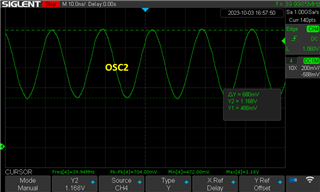
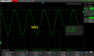
Attached are our schematic and the plots of OSC1 and OSC2

  • Hi Igor,

    Do you by chance know how much capacitance your passive scope probe has?  I'm just trying to get a feel for what might be added when you are measuring the OSC2 waveform.  The plot shows a min voltage of 472mV which is much higher than the typical 100mV and 150mV max single-ended detection compartor threshold. 

    You are correct that increasing the capacitance will shift the frequency, but generally this is not enough to violate the clock tolerance criteria in the CAN specification.  However, the allowed tolerance also decreases as you increase the bit rate, so this is somewhat application specific.

    The voltage levels are set based on the resistance and reactance of the components that create some voltage divider type of effects on the common mode levels.  The OSC1 side is generally lower than the OSC2 side, and this is also visible in your plots.  Some adjustment can be made to these common mode levels by simply adjusting the ratio of capacitance on the two sides of the crystal.  Increasing the capacitance on the OSC2 side and decreasing the amount on the OSC1 side by the same amount will keep the total capacitance the same, but increase the common mode voltage level of the OSC2 side.

    So, without adding a series resistor you could:

    1.) Try to increase both cap values equally and measure/verify the clock frequency shift is still within the CAN specification limits for your application

    2.) Shift capacitance to the OSC2 side by making the C12 = 10pF, and C11 = 6pF, or even C12 = 12pF and C11 = 4pF, etc. Then evaluate and verify the performance and check for stability.

    Let me know your results.

    Regards,

    Jonathan

  • Hi Igor,

    If you have not seen already, more information can be found in the TCAN455x Clock Optimization and Design Guidelines application note (Link).

    Regards,

    Jonathan

  • Thank you, yes I did see the appnote but somehow missed the recommendation to have a placeholder Rd .
    As far as measurement- I am using a Siglent  SDS1104X-E scope with PP510 passive probes in 10X mode (https://assets.testequity.com/te1/Documents/pdf/siglent/siglent-probe-series-datasheet.pdf)
    so likely adding a non-insignificant amount of capacitance (18.5 pF-22.5 pF, 10M) to the circuit. 
    Seems I need proper tools to even look at this without affecting the results, something like an active probe

  • Yes, the scope probes are going to add significant capacitance during measurement and you would not be able to observe a disruption to the clock circuit when the scope probe is attached.  Low capacitance active probes are needed to reduce measurement error for these type of measurements.

    Do you have access and probe the GPIO1 pin during your testing?  Also, do you know under what conditions your communications start to fail, such as higher/lower temperature, etc.?

    Regards,

    Jonathan

  • We do have a test point on GPIO1, but the datasheet seems to have removed any mention of how to use if to output Clock on it. In fact revision history says " Deleted CLKOUT from the GPIO1 circuit in Figure 8-2". What do we need to do to output clock there?
    The weird thing is we are seeing issues in the absence of temperature extremes, at room temp

  • I have just sent you some information through your registered email address.  Typically we see an issue that is temperature related, or at least more frequent with an increase or change in temperature, so if you do not see this type of behavior, then there may be some other issue causing your communication errors.  Also, try to change the capacitance and see if the communication errors increase or decrease in frequency which would help confirm whether this is or is not a clock related issue.

    Regards,

    Jonathan