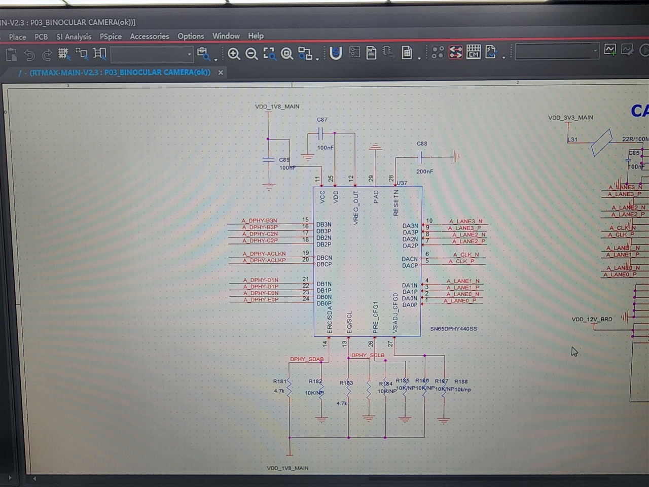
We are currently working to integrate the SN65DPHY440 MIPI Repeater IC into our design and ran into the issue with lane 0 which had been brought up before.
1. We tried setting the registers to the following recommendations:
Write Register 0x50 with 8’h01 //Override enable for HS TX path
Write Register 0x51 with 8’h01 //HS TX path enabled.
Write Register 0x61 with 8’h1E // Disable LP path for lane 0
Write Register 0x70 with 8’h01 //Override enable for HS RX path
Write Register 0x71 with 8’h01 // HS RX path enabled.
And we are still seeing erroneous data read from lane 0 which we feel is due to the other lanes transitioning properly from LP mode to HS while lane 0 remains in HS mode.
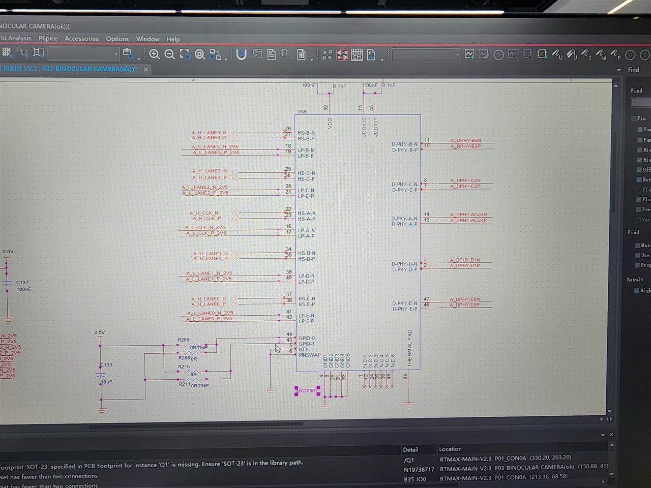
We then tried:
Write Register 0x50 with 8’h1F //Override enable for HS TX path
Write Register 0x51 with 8’h1F //HS TX path enabled.
Write Register 0x61 with 8’h00 // Disable LP path for all lanes
Write Register 0x70 with 8’h1F //Override enable for HS RX path
Write Register 0x71 with 8’h1F // HS RX path enabled.
And we get erroneous data read on all lanes.
Any recommendations to fix this issue?
2. Also, we are currently planning to add a MIPI DPHY MC20901 IC from Meticom which will be connected to the TX end of the SN65DPHY440, I wanted to enquire if this would solve the issue of lane 0 by providing an unterminated connection to the lane 0 TX.
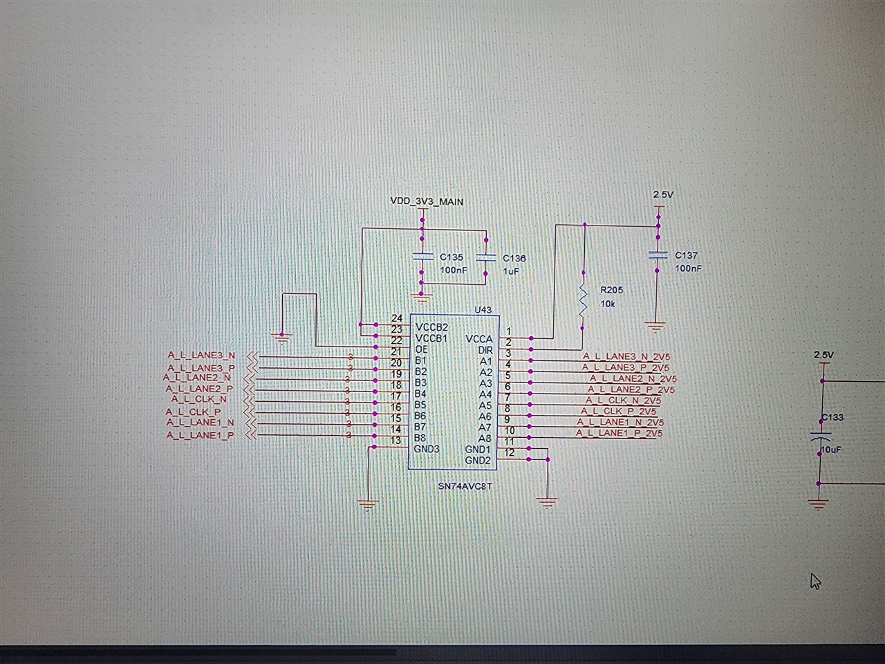
3. Would it be possible to have two SN65DPHY440 connected in parallel, with the same clock source, but with lane 0 unused?