This thread has been locked.

If you have a related question, please click the "Ask a related question" button in the top right corner. The newly created question will be automatically linked to this question.

DP83TD510E: link problem of the phy chip in linux

Part Number: DP83TD510E

Hello:

I am having problems using DP83TD510E.
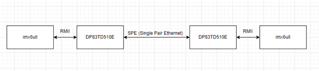
Environment:

DP83TD510E works in rmii slave mode. Soc provides a 50Mhz clock to the xi pod.

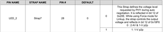
CRS_DV/RX_DV Pin 18 is configured as CRS_DV (default).

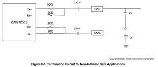
Receiver with tapping at 50 Ω (Recommended).

The id of the phy chip is set to 0.

linux system from the following github link.

https://github.com/nxp-imx/linux-imx/blob/lf-6.1.y/drivers/net/phy/dp83td510.c

My configuration in the device tree is as follows.

&fec1 {
pinctrl-names = "default";
pinctrl-0 = <&pinctrl_enet1>;
phy-mode = "rmii";
phy-handle = <&ethphy0>;
phy-reset-gpios = <&gpio1 1 GPIO_ACTIVE_LOW>;
phy-reset-duration = <2>;
status = "okay";
};

&fec2 {
......
mdio {
#address-cells = <1>;
#size-cells = <0>;

ethphy0: ethernet-phy@0 {
compatible = "ethernet-phy-id2000.0180";
reg = <0>;
clocks = <&clks IMX6UL_CLK_ENET_REF>;
clock-names = "rmii-ref";
};
......
};
};
......
pinctrl_enet1: enet1grp {
fsl,pins = <
MX6UL_PAD_ENET1_RX_EN__ENET1_RX_EN 0x1b0b0
MX6UL_PAD_ENET1_RX_ER__ENET1_RX_ER 0x1b0b0
MX6UL_PAD_ENET1_RX_DATA0__ENET1_RDATA00 0x1b0b0
MX6UL_PAD_ENET1_RX_DATA1__ENET1_RDATA01 0x1b0b0
MX6UL_PAD_ENET1_TX_EN__ENET1_TX_EN 0x1b0b0
MX6UL_PAD_ENET1_TX_DATA0__ENET1_TDATA00 0x1b0b0
MX6UL_PAD_ENET1_TX_DATA1__ENET1_TDATA01 0x1b0b0
MX6UL_PAD_ENET1_TX_CLK__ENET1_REF_CLK1 0x4001b039
MX6UL_PAD_GPIO1_IO01__GPIO1_IO01 0xb0
>;
};
......

Fullscreen
1
2
3
4
5
6
7
8
9
10
11
12
13
14
15
16
17
18
19
20
21
&fec1 {
pinctrl-names = "default";
pinctrl-0 = <&pinctrl_enet1>;
phy-mode = "rmii";
phy-handle = <&ethphy0>;
phy-reset-gpios = <&gpio1 1 GPIO_ACTIVE_LOW>;
phy-reset-duration = <2>;
status = "okay";
};
&fec2 {
......
mdio {
#address-cells = <1>;
#size-cells = <0>;
ethphy0: ethernet-phy@0 {
compatible = "ethernet-phy-id2000.0180";
reg = <0>;
clocks = <&clks IMX6UL_CLK_ENET_REF>;
clock-names = "rmii-ref";

Product test is shown below.

Problem:

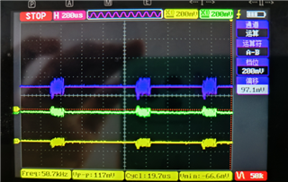
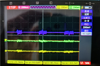
The DP83TD510E is always in the Link is down state, and I don't know how to deal with it. The DP83TD510E has been registered.

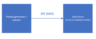
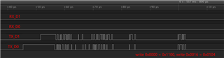
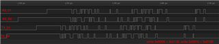
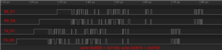
I tried to test Loopback Modes, but I still don't know how to handle it.

I tried to read the external register, but I didn't know how to read it, something like 0x201.

Thanks.

Best regards
Kailyn
  • Hi Kailyn,

    Please share a register dump from addresses 0 to 1F. This FAQ is a useful reference if you are interfacing with the PHY in a Linux terminal:

    https://e2e.ti.com/support/interface-group/interface/f/interface-forum/1164499/faq-how-to-read-and-write-ethernet-phy-registers-using-a-linux-terminal

    If you have access to a packet generator, the following test is recommended to validate the MDI and internal signal path:

    If the packet generator receives the same data looped back without error, then the MDI and internal signal path is valid, with the issue isolated to the MAC-side.

    Reverse loopback is set by writing address 0x0016 = 0x0110

    Thank you,

    Evan

  • Hi Evan,

    Thanks for support.

    The values of registers 0 to 1F are as follows.

    Register 0x00 = read phy addr: 0x0 reg: 0x0 value : 0x1100
    Register 0x01 = read phy addr: 0x0 reg: 0x1 value : 0x149
    Register 0x02 = read phy addr: 0x0 reg: 0x2 value : 0x2000
    Register 0x03 = read phy addr: 0x0 reg: 0x3 value : 0x181
    Register 0x04 = read phy addr: 0x0 reg: 0x4 value : 0x0
    Register 0x05 = read phy addr: 0x0 reg: 0x5 value : 0x0
    Register 0x06 = read phy addr: 0x0 reg: 0x6 value : 0x0
    Register 0x07 = read phy addr: 0x0 reg: 0x7 value : 0x0
    Register 0x08 = read phy addr: 0x0 reg: 0x8 value : 0x0
    Register 0x09 = read phy addr: 0x0 reg: 0x9 value : 0x0
    Register 0x0A = read phy addr: 0x0 reg: 0xa value : 0x0
    Register 0x0B = read phy addr: 0x0 reg: 0xb value : 0x0
    Register 0x0C = read phy addr: 0x0 reg: 0xc value : 0x0
    Register 0x0D = read phy addr: 0x0 reg: 0xd value : 0x401f
    Register 0x0E = read phy addr: 0x0 reg: 0xe value : 0x6000
    Register 0x0F = read phy addr: 0x0 reg: 0xf value : 0x0
    Register 0x10 = read phy addr: 0x0 reg: 0x10 value : 0x0
    Register 0x11 = read phy addr: 0x0 reg: 0x11 value : 0x28
    Register 0x12 = read phy addr: 0x0 reg: 0x12 value : 0x0
    Register 0x13 = read phy addr: 0x0 reg: 0x13 value : 0x2100
    Register 0x14 = read phy addr: 0x0 reg: 0x14 value : 0x0
    Register 0x15 = read phy addr: 0x0 reg: 0x15 value : 0x0
    Register 0x16 = read phy addr: 0x0 reg: 0x16 value : 0x100
    Register 0x17 = read phy addr: 0x0 reg: 0x17 value : 0x40a1
    Register 0x18 = read phy addr: 0x0 reg: 0x18 value : 0x443
    Register 0x19 = read phy addr: 0x0 reg: 0x19 value : 0x0
    Register 0x1A = read phy addr: 0x0 reg: 0x1a value : 0x0
    Register 0x1B = read phy addr: 0x0 reg: 0x1b value : 0x0
    Register 0x1C = read phy addr: 0x0 reg: 0x1c value : 0x0
    Register 0x1D = read phy addr: 0x0 reg: 0x1d value : 0x0
    Register 0x1E = read phy addr: 0x0 reg: 0x1e value : 0x0
    Register 0x1F = read phy addr: 0x0 reg: 0x1f value : 0x0

    I do not have a packet generator at the moment, but will consider the offer.

    Thanks.

  • Hi Evan,

    I modified the hardware drop-down. The value of the register is changed.

    The values of registers 0 to 1F are as follows.

    Register 0x00 = read phy addr: 0x0 reg: 0x0 value : 0x1100
    Register 0x01 = read phy addr: 0x0 reg: 0x1 value : 0x149
    Register 0x02 = read phy addr: 0x0 reg: 0x2 value : 0x2000
    Register 0x03 = read phy addr: 0x0 reg: 0x3 value : 0x181
    Register 0x04 = read phy addr: 0x0 reg: 0x4 value : 0x0
    Register 0x05 = read phy addr: 0x0 reg: 0x5 value : 0x0
    Register 0x06 = read phy addr: 0x0 reg: 0x6 value : 0x0
    Register 0x07 = read phy addr: 0x0 reg: 0x7 value : 0x0
    Register 0x08 = read phy addr: 0x0 reg: 0x8 value : 0x0
    Register 0x09 = read phy addr: 0x0 reg: 0x9 value : 0x0
    Register 0x0A = read phy addr: 0x0 reg: 0xa value : 0x0
    Register 0x0B = read phy addr: 0x0 reg: 0xb value : 0x0
    Register 0x0C = read phy addr: 0x0 reg: 0xc value : 0x0
    Register 0x0D = read phy addr: 0x0 reg: 0xd value : 0x401f
    Register 0x0E = read phy addr: 0x0 reg: 0xe value : 0x2402
    Register 0x0F = read phy addr: 0x0 reg: 0xf value : 0x0
    Register 0x10 = read phy addr: 0x0 reg: 0x10 value : 0x0
    Register 0x11 = read phy addr: 0x0 reg: 0x11 value : 0x28
    Register 0x12 = read phy addr: 0x0 reg: 0x12 value : 0x0
    Register 0x13 = read phy addr: 0x0 reg: 0x13 value : 0x100
    Register 0x14 = read phy addr: 0x0 reg: 0x14 value : 0x0
    Register 0x15 = read phy addr: 0x0 reg: 0x15 value : 0x0
    Register 0x16 = read phy addr: 0x0 reg: 0x16 value : 0x100
    Register 0x17 = read phy addr: 0x0 reg: 0x17 value : 0x40a1
    Register 0x18 = read phy addr: 0x0 reg: 0x18 value : 0x443
    Register 0x19 = read phy addr: 0x0 reg: 0x19 value : 0x0
    Register 0x1A = read phy addr: 0x0 reg: 0x1a value : 0x0
    Register 0x1B = read phy addr: 0x0 reg: 0x1b value : 0x0
    Register 0x1C = read phy addr: 0x0 reg: 0x1c value : 0x0
    Register 0x1D = read phy addr: 0x0 reg: 0x1d value : 0x0
    Register 0x1E = read phy addr: 0x0 reg: 0x1e value : 0x0
    Register 0x1F = read phy addr: 0x0 reg: 0x1f value : 0x0

    If only one device is powered on. I writing address 0x0016 = 0x0108. DP83TD510E link is Up.

    Then I power on another device. DP83TD510E link is Down. I don't understand the reason for this phenomenon, maybe this will help solve the problem.

    Thanks.

  • Hi Liangtao,

    The register configuration looks good to me.

    If only one device is powered on. I writing address 0x0016 = 0x0108. DP83TD510E link is Up.

    Then I power on another device. DP83TD510E link is Down.

    0x0016 = 0x0108 programs the device in analog loopback mode. In this mode, link will always be up as the device links with itself on the MDI side to loop the data back internally.

    The cause of this issue is still unclear to me, could you share a block diagram and schematic file? (Email to e-mayhew@ti.com for private share)

    Are you able to send and check packets on the SoC used for the MAC connection? If so, please write 0x0016 = 0x0104 to set digital loopback and verify the SoC receives the same data transmitted.

    Thank you,

    Evan

  • Hi Evan,

    Schematics have been sent by email.

    I don't know if there is any way to easily verify mac data on linux, so I use tcpdump to grab the data.

    I forcibly modified phydev->link = 1 in the driver, then I got the following log.

    [root@test:~]# ping 192.168.0.11
    PING 192.168.0.11 (192.168.0.11): 56 data bytes
    00:04:40.682556 ARP, Request who-has 192.168.0.11 tell 192.168.0.22, length 28
    00:04:41.760181 ARP, Request who-has 192.168.0.11 tell 192.168.0.22, length 28
    00:04:42.800204 ARP, Request who-has 192.168.0.11 tell 192.168.0.22, length 28
    00:04:44.684508 ARP, Request who-has 192.168.0.11 tell 192.168.0.22, length 28
    00:04:45.760221 ARP, Request who-has 192.168.0.11 tell 192.168.0.22, length 28

    When I write 0x0000 = 0x5100, 0x0016 = 0x0100, then I got the following log.

    [root@test:~]# ping 192.168.0.11
    PING 192.168.0.11 (192.168.0.11): 56 data bytes
    00:05:35.289721 ARP, Request who-has 192.168.0.11 tell 192.168.0.22, length 28
    00:05:35.291118 ARP, Request who-has 192.168.0.11 tell 192.168.0.22, length 46
    00:05:36.320214 ARP, Request who-has 192.168.0.11 tell 192.168.0.22, length 28
    00:05:36.321432 ARP, Request who-has 192.168.0.11 tell 192.168.0.22, length 46
    00:05:37.360227 ARP, Request who-has 192.168.0.11 tell 192.168.0.22, length 28
    00:05:37.361470 ARP, Request who-has 192.168.0.11 tell 192.168.0.22, length 46

    When I write 0x0000 = 0x1100, write 0x0016 = 0x0104; then I got the following log.

    [root@test:~]# ping 192.168.0.11
    PING 192.168.0.11 (192.168.0.11): 56 data bytes
    00:07:04.592268 ARP, Request who-has 192.168.0.11 tell 192.168.0.22, length 28
    00:07:05.600203 ARP, Request who-has 192.168.0.11 tell 192.168.0.22, length 28
    00:07:06.640279 ARP, Request who-has 192.168.0.11 tell 192.168.0.22, length 28
    00:07:08.594406 ARP, Request who-has 192.168.0.11 tell 192.168.0.22, length 28

    When I write 0x0000 = 0x1100, write 0x0016 = 0x0108; then I got the following log.

    [root@test:~]# ping 192.168.0.11
    PING 192.168.0.11 (192.168.0.11): 56 data bytes
    00:32:47.532609 ARP, Request who-has 192.168.0.11 tell 192.168.0.22, length 28
    00:32:47.533775 ARP, Request who-has 192.168.0.11 tell 192.168.0.22, length 46
    00:32:48.568965 ARP, Request who-has 192.168.0.11 tell 192.168.0.22, length 28
    00:32:48.570214 ARP, Request who-has 192.168.0.11 tell 192.168.0.22, length 46
    00:32:49.608941 ARP, Request who-has 192.168.0.11 tell 192.168.0.22, length 28
    00:32:49.610175 ARP, Request who-has 192.168.0.11 tell 192.168.0.22, length 46

    Does the above indicate that I cannot receive the same data when I write 0x0016 = 0x0104 to set digital loopback ?

    At the same time, I used a logic analyzer to capture the data(write 0x0000 = 0x1100, write 0x0016 = 0x0104).

    write 0x0000 = 0x5100, write 0x0016 = 0x0100

    write 0x0000 = 0x1100, write 0x0016 = 0x0108

    Thanks.

  • Hi Liangtao,

    I'm not certain how to interpret the ping log, but the logic analyzer capture appears to indicate the MAC connection is valid with the data being looped back.

    Thank you for performing this test and sharing the schematic. I will review and discuss with the team for possible root causes on MDI-side link failure (follow-up by EOD tomorrow).

    Sincerely,

    Evan

  • Hi Evan,

    I appreciate the effort. Look forward to finding out what the problem is.

    Thanks.

  • Hi Liangtao,

    Is there any activity when probing the MDI lines?

    Which termination circuit is intended? The schematic does not show a CMC or series capacitors on the MDI line, this may cause link issues:

    Thank you,

    Evan

  • Hi Evan,

    Below is the signal I measured on MDI lines. Vp-p 235mv.

    CMC and series capacitors removed due to commissioning issues.

    If we use the following terminal circuit is there a problem?

    Thanks.

  • Hi Evan,

    The schematics have been sent again by email.

    I used two new boards with CMC and series capacitors on the MDI line,  But the problem is the same.

    The new board seems to pick up a smaller signal.

    Thanks.

  • Hi Liangtao,

    The termination scheme in the most recent schematic shared over email looks good.

    When you noted link is up when removing C29 and C30, how are you determining link status, and was the device in analog loopback mode (0x16 = 0x108)?

    We do not recommend using any loopback mode for normal operation - these modes are intended for isolating link issues to a specific part of the signal chain.

    Which PHY is being used as the link partner for this application?

    Are there any working link cases while the 510 is not programmed in loopback? If so, please share the block diagram and device configuration for this case.

    Thank you,

    Evan

  • Hi Evan,

    When you noted link is up when removing C29 and C30, how are you determining link status, and was the device in analog loopback mode (0x16 = 0x108)?

    On a new device,i writing address 0x0016 = 0x0108,removing C29 and C30, the new device will be in link up state.

    I use the iplink tool to determine if the device is in the link state.

    Kernel logs can also determine if the device is in the link state, because the DP83TD510E_PHY_STS register of the phy is read every second in the driver.

    Which PHY is being used as the link partner for this application?

    DP83TD510E is being used as the link partner for this application.

    Are there any working link cases while the 510 is not programmed in loopback? If so, please share the block diagram and device configuration for this case.

    There are no working link cases while the 510 is not programmed in loopback.

    Thanks.

  • Hi Liangtao,

    The most recent schematic shows both a 2.49k PU and PD on Strap7 - please remove one of these resistors on both 510s and ensure they are strapped into the same swing mode.

    It's possible the two 510s are programmed for different swing levels (1vpp vs. 2.4vpp), which may cause link issues on the MDI side.

    Please also share a register dump from addresses 0x0 to 0x38E7 for both 510s so I may confirm the configurations are compatible for MDI link.

    Thank you,

    Evan

  • Hi Evan,

    The most recent schematic shows both a 2.49k PU and PD on Strap7 - please remove one of these resistors on both 510s and ensure they are strapped into the same swing mode.

    Yes, as mentioned in the email, I removed the 2.49k PU.

    Remove D13、R89.  Ensure that Strap7 = 0.

    Please also share a register dump from addresses 0x0 to 0x38E7 for both 510s so I may confirm the configurations are compatible for MDI link.

    I tried to read the external register, but I didn't know how to read it, something like 0x38E7.

    The values of registers 0 to 1F are as follows.

    Register 0x00 = read phy addr: 0x0 reg: 0x0 value : 0x1100
    Register 0x01 = read phy addr: 0x0 reg: 0x1 value : 0x149
    Register 0x02 = read phy addr: 0x0 reg: 0x2 value : 0x2000
    Register 0x03 = read phy addr: 0x0 reg: 0x3 value : 0x181
    Register 0x04 = read phy addr: 0x0 reg: 0x4 value : 0x0
    Register 0x05 = read phy addr: 0x0 reg: 0x5 value : 0x0
    Register 0x06 = read phy addr: 0x0 reg: 0x6 value : 0x0
    Register 0x07 = read phy addr: 0x0 reg: 0x7 value : 0x0
    Register 0x08 = read phy addr: 0x0 reg: 0x8 value : 0x0
    Register 0x09 = read phy addr: 0x0 reg: 0x9 value : 0x0
    Register 0x0A = read phy addr: 0x0 reg: 0xa value : 0x0
    Register 0x0B = read phy addr: 0x0 reg: 0xb value : 0x0
    Register 0x0C = read phy addr: 0x0 reg: 0xc value : 0x0
    Register 0x0D = read phy addr: 0x0 reg: 0xd value : 0x401f
    Register 0x0E = read phy addr: 0x0 reg: 0xe value : 0x2101
    Register 0x0F = read phy addr: 0x0 reg: 0xf value : 0x0
    Register 0x10 = read phy addr: 0x0 reg: 0x10 value : 0x0
    Register 0x11 = read phy addr: 0x0 reg: 0x11 value : 0x28
    Register 0x12 = read phy addr: 0x0 reg: 0x12 value : 0x0
    Register 0x13 = read phy addr: 0x0 reg: 0x13 value : 0x100
    Register 0x14 = read phy addr: 0x0 reg: 0x14 value : 0x0
    Register 0x15 = read phy addr: 0x0 reg: 0x15 value : 0x0
    Register 0x16 = read phy addr: 0x0 reg: 0x16 value : 0x100
    Register 0x17 = read phy addr: 0x0 reg: 0x17 value : 0x40a1
    Register 0x18 = read phy addr: 0x0 reg: 0x18 value : 0x443
    Register 0x19 = read phy addr: 0x0 reg: 0x19 value : 0x0
    Register 0x1A = read phy addr: 0x0 reg: 0x1a value : 0x0
    Register 0x1B = read phy addr: 0x0 reg: 0x1b value : 0x0
    Register 0x1C = read phy addr: 0x0 reg: 0x1c value : 0x0
    Register 0x1D = read phy addr: 0x0 reg: 0x1d value : 0x0
    Register 0x1E = read phy addr: 0x0 reg: 0x1e value : 0x0
    Register 0x1F = read phy addr: 0x0 reg: 0x1f value : 0x0

    Thanks.

  • Hi Liangtao,

    Please refer to this FAQ and MMD mapping for the extended register procedure:

    https://e2e.ti.com/support/interface-group/interface/f/interface-forum/1133146/faq-dp83tg720s-q1-how-to-read-or-write-registers-in-extended-register-space-of-ethernet-phy

    If the full register dump from 0x0 to 0x38E7 is not feasible with this procedure, here are the key registers that would be useful to see for both 510s attempting to link:

    0x12A, 0x12B, 0x12D, 0x12E, 0x12F, 0x130, 0x200, 0x201, 0x20E, 0x20F, 0x3000, 0x18F6, 0x18F7, 0x38E7

    Please share two register dumps for each 510, while they are connected and there is activity on the MDI line.

    Are you seeing any LED activity while the MDI line is active? LED_0 (D15) indicates link and RX/TX activity by default.

    Thank you,

    Evan

  • Hi Evan,

    Are you seeing any LED activity while the MDI line is active? LED_0 (D15) indicates link and RX/TX activity by default.

    I didn't see any led activity when the MDI line was active. LED_0 is always on.

    The key registers of the two devices are as follows, all the registers are attached.

    # device 1
    read phy addr: 0x0 reg: 0x012A value : 0x0000
    read phy addr: 0x0 reg: 0x012B value : 0x0000
    read phy addr: 0x0 reg: 0x012D value : 0x0000
    read phy addr: 0x0 reg: 0x012E value : 0x0000
    read phy addr: 0x0 reg: 0x012F value : 0x0000
    read phy addr: 0x0 reg: 0x0130 value : 0x0000
    read phy addr: 0x0 reg: 0x0200 value : 0x1000
    read phy addr: 0x0 reg: 0x0201 value : 0x0008
    read phy addr: 0x0 reg: 0x020E value : 0xB000
    read phy addr: 0x0 reg: 0x020F value : 0x0000
    read phy addr: 0x0 reg: 0x3000 value : 0x0000
    read phy addr: 0x0 reg: 0x38E7 value : 0x0000
    read phy addr: 0x0 reg: 0x18F6 value : 0x0000
    read phy addr: 0x0 reg: 0x18F7 value : 0x0000
    
    # device 2
    read phy addr: 0x0 reg: 0x012A value : 0x0000
    read phy addr: 0x0 reg: 0x012B value : 0x0000
    read phy addr: 0x0 reg: 0x012D value : 0x0000
    read phy addr: 0x0 reg: 0x012E value : 0x0000
    read phy addr: 0x0 reg: 0x012F value : 0x0000
    read phy addr: 0x0 reg: 0x0130 value : 0x0000
    read phy addr: 0x0 reg: 0x0200 value : 0x1000
    read phy addr: 0x0 reg: 0x0201 value : 0x0008
    read phy addr: 0x0 reg: 0x020E value : 0xB000
    read phy addr: 0x0 reg: 0x020F value : 0x0000
    read phy addr: 0x0 reg: 0x3000 value : 0x0000
    read phy addr: 0x0 reg: 0x38E7 value : 0x0000
    read phy addr: 0x0 reg: 0x18F6 value : 0x0000
    read phy addr: 0x0 reg: 0x18F7 value : 0x0000
    reg_dump_dev2.txtreg_dump_dev1.txt

    Thanks.

  • Hi Liangtao,

    Thank you for sharing the full register dump.

    The MDI output swing should be around 2.4V ptp, it seems like there is some connection on the line reducing the voltage swing such that the 510s cannot link.

    Please measure and share the MDI capture again after removing C28, C31, and L3.

    Is this a PoDL application? If so, are you able to power the other board externally without L3?

    Thank you,

    Evan

  • Hi Evan,

    I found that there was something wrong with the code of the key registers captured yesterday. After modification, I re-captured the key register as follows. But full register dump in txt file is normal.

    # device 1
    read phy addr: 0x0 reg: 0x012A value : 0x0000
    read phy addr: 0x0 reg: 0x012B value : 0x0000
    read phy addr: 0x0 reg: 0x012D value : 0x0000
    read phy addr: 0x0 reg: 0x012E value : 0x0000
    read phy addr: 0x0 reg: 0x012F value : 0x0000
    read phy addr: 0x0 reg: 0x0130 value : 0x0000
    read phy addr: 0x0 reg: 0x0200 value : 0x1000
    read phy addr: 0x0 reg: 0x0201 value : 0x0008
    read phy addr: 0x0 reg: 0x020E value : 0xB000
    read phy addr: 0x0 reg: 0x020F value : 0x0000
    read phy addr: 0x0 reg: 0x3000 value : 0x0000
    read phy addr: 0x0 reg: 0x38E7 value : 0x0000
    read phy addr: 0x0 reg: 0x18F6 value : 0x1000
    read phy addr: 0x0 reg: 0x18F7 value : 0x3000
    
    # device 2
    read phy addr: 0x0 reg: 0x012A value : 0x0000
    read phy addr: 0x0 reg: 0x012B value : 0x0000
    read phy addr: 0x0 reg: 0x012D value : 0x0000
    read phy addr: 0x0 reg: 0x012E value : 0x0000
    read phy addr: 0x0 reg: 0x012F value : 0x0000
    read phy addr: 0x0 reg: 0x0130 value : 0x0000
    read phy addr: 0x0 reg: 0x0200 value : 0x1000
    read phy addr: 0x0 reg: 0x0201 value : 0x0008
    read phy addr: 0x0 reg: 0x020E value : 0xB000
    read phy addr: 0x0 reg: 0x020F value : 0x0000
    read phy addr: 0x0 reg: 0x3000 value : 0x0000
    read phy addr: 0x0 reg: 0x38E7 value : 0x0000
    read phy addr: 0x0 reg: 0x18F6 value : 0x1000
    read phy addr: 0x0 reg: 0x18F7 value : 0x3000

    The one marked NC on the schematic is not welded, so C28 and C31 are not welded; L3, as stated in the email, has been removed; I re-captured the MDI signal as shown below:

    case 1:Only one device is powered on.

    The yellow signal is 1-PD_P to ground, the green signal is 1-PD_N to ground, and the purple signal is the yellow signal minus the green signal.

    case 2:The two devices are powered on independently and connected using twisted pair cables.

    Is this a PoDL application? If so, are you able to power the other board externally without L3?

    This is a PoDL application, but in order to debug phy, L3, D8, D9, D10, D11, D12 are temporarily removed, and the two boards are powered independently.

    I don't understand what 2.4V ptp means, is vpp == 2.4v?

    Thanks.

  • Hi Evan,

    In the schematic, R30 and R51 are 49.9Ω, but my measuring board is 50kΩ, so I replaced the resistance from 50kΩ to 49.9Ω. After this modification, the phy will link up successfully.

    I really appreciate your professional and patient support for so many days.

    Thanks a lot.

  • Hi Evan,

    When I use the power supply in pdf, device 1 powers device 2, the phy chip is always in link down state.

    Is there a problem with the design in pdf?

    Do you have a PoDL application reference design schematic?

    Thanks.PoDL_to_ti.pdf

  • Hi Liangtao,

    I'm glad you found the cause of the issue, thank you for sharing all of the information requested for debug.

    I am checking with the team if we have a PoDL reference schematic to share, please expect a follow-up on this by tomorrow.

    Thanks,

    Evan

  • Hi Liangtao,

    We will continue the PoDL discussion over email.

    Thank you,

    Evan

  • Hi Evan,
    Thank you for your support.