This thread has been locked.

If you have a related question, please click the "Ask a related question" button in the top right corner. The newly created question will be automatically linked to this question.

DP83867IR: Device not responding

Part Number: DP83867IR

Hi,

We are using the part DP83867IRRGZ in our board.

We observed that the Crystal connected (ABM8G-25.000MHZ) to the PHY is not providing the clock input.

We tried programming the MDIO and observed that the PHY is also not responding. Checked the PHY reset input, PHY is out of reset.

Can you please help with possible causes for the issue?

Thanks & Regards,

Nanjunda M

  • Hi Nanjunda,

    Our PHY will not function if it is not receiving an input clock. The clock is essentially the heartbeat, so it is an absolute must that the clock issue gets resolved before attempting anything else.

    Please reference the following document, I hope that this can help you in the future.

    DP83867 Troubleshooting Guide

    Regards,

    Alvaro

  • Hi Alvaro,

    Beside the input clock is there any other possible issues that can raise the device not respond?

    Thanks & Regards,

    Nanjunda M

  • Hi Nanjunda,

    There are, but this should be the first check. Can you probe the CLKOUT pin and confirm you see a waveform? If yes, then the PHY is alive and register access via MDC/MDIO should be available.

    Regards,

    Alvaro

  • Hi Alvaro,

    We provided the external clock and now we are able to see 25MHz clock output on CLKOUT pin.

    But we see that MDIO response are 00 always. Can you please let me know how can we proceed?

    Thanks & Regards,

    Nanjunda M

  • Hi Nanjunda,

    Glad to hear we're able to get the 25 MHz from CLKOUT. The next thing I want to confirm is if the MDIO line has a 2.2 kΩ Pull up resistor connected to VDDIO, this is necessary for register access.

    How are you currently trying to access the registers? Is it via a Processor?

    Regards,

    Alvaro

  • Hi Alvaro,

    MDIO has a pullup of 1.5K Ohm to VDDIO.

    We are trying access registers from a Zynq SOC, which supports standard 2.5MHz MDC-MDIO interface.

    Thanks & Regards,

    Nanjunda M

  • Hi Nanjunda,

    A 1.5 kΩ PU on MDIO should be okay. Next we can check if the Zynq SOC is providing the 2.5 MHz MDC to the PHY. Is it possible to probe the MDC/MDIO lines?

    Would also recommend double checking the strapping on the PHY to confirm the PHY_ID. If the SOC has the incorrect PHY_ID then this would probably be the reason why Register Access isn't working.

    Regards,

    Alvaro

  • HI Alvaro,

    We have checked that MDC is 2.5MHz.

    we have set the PHY address to 0, that means the straps are set to be open connection as per the datasheet. Please correct me if I'm wrong.

    Thanks & Regards,

    Nanjunda M

  • Hi Nanjunda,

    Correct, leaving RX_D0 and RX_D2 as Open will set the PHY address to 0. Can we confirm these straps by probing them during power up? Can we try using all possible PHY_IDs to rule out this issue? 

    Also, I will be out of office from Nov 23rd-Nov 29th. Expect no responses until Nov 30th.

    Regards,

    Alvaro

  • Hi Alvaro,

    Tried with different PHY IDs and we see 0 as response for all register reads.

    Can you please help us to debug further? 

    Thanks & Regards,
    Nanjunda M

  • Hi Nanjunda,

    Thank you for patiently waiting for my response.

    I want to summarize the issue so far and see if we can maybe re-check a few things.

    1. Is the PHY alive?
      1. Probe CLKOUT
        1. 25 MHz signal was seen Heavy check mark
      2. Link LED
        1. Do you have any LEDs connected?
        2. Do you see link up when you connect the ethernet cable to the RJ-45 Connector?
      3. Throughput/Ping Test
        1. Are you able to send data/ping?
    2. Schematic/Layout
      1. Does the MDIO line have a 2.2 kΩ PU to VDDIO?
        1. It has a 1.5 kΩ PU to VDDIO
          1. This is defined by IEEE and is okay Heavy check mark
      2. Is the Processor providing MDC?
        1. Yes, it is providing a 2.5 MHz Clock Heavy check mark
      3. Is the PHY Address strapped correctly?
        1. RX_D0 & RX_D2 are left floating, this would make the PHY_ADD = 0
        2. What MAC Interface are you using? Would you be able to send me a PDF of the Ethernet portion of your schematic?

    Regards,

    Alvaro

  • Hi Alvaro,

    Sorry for the delayed response.

    1.b.A - Yes, LED2 & LED1 LEDs are connected to the Magjack

    1.b.B - No, i do not see any link up LED glowing on the RJ45 connector

    1.c.A - No. not able to as its not connecting.

    2.c.A - Correct

    2.c.B - We are using the Zynq Ultrascle+ FPGA PS at the MAC. PFA schematics.

    Thanks & Regards,

    Nanjunda M

  • Hi Nanjunda,

    I reviewed your schematics and I don't see any issues with it. I want to direct you again to the troubleshooting guide, specifically section 3.4.

    Could you probe the Power, Reset, CLKOUT, MDC, and MDIO during boot-up and again once in steady state?

    DP83867 Troubleshooting Guide

    Regards,

    Alvaro

  • Hi Alvaro,

    Sorry for the delayed response.

    We have a delayed reset sequence due to clock input we have provided.

    We are providing the reset from the FPGA (after approx. 1min after processor bootup) and is provided once the clock input is provided to the Ethernet PHY. (Provided by clock generator after 30seconds of powers are stable). The Drivers will be initiated manually by commands. 

    Please let me know if this can cause any issue.

    Thanks & Regards,

    Nanjunda M

  • Hi Nanjunda,

    To confirm my understanding

    1. you are allowing the FPGA to bootup first
      1. then the FPGA is asserting a low signal onto the reset pin of the PHY.
    2. Power and Clock boot up as well, and you wait ~30 seconds for them to be stable
      1. This is excellent, 30 seconds might be overkill, but essentially we want a stable clock prior to power.
    3. After Power and Clock is stable, the FPGA releases the PHY from reset
    4. Drivers are manually initiated after steps 1-3

    This is completely fine, are you able to read and write registers now?

    Regards,

    Alvaro

  • Hi Alvaro,

    No, we are not able to read and write. We see still there is no response from the PHY on MDIO pin.

    Thanks & Regards,

    Nanjunda M

  • Hi Nanjunda,

    Alvaro is currently out of office. He will reach back to you right after he get back to the office.

    --

    Regards,

    Hillman Lin

  • Hi Alvaro,

    Found an issue with the PHY.

    Whenever the Phy gets clock input, it seems to be sinking the MDIO pin and the MDIO pin voltage drops to 1.1V when the MAC is communicating with the PHY. However, when the PHY is not active, i.e. when clock input is not present and the MDIO is driven, the voltage of MDIO is at 1.8V.

    Any idea what could cause such behavior of Ethernet PHY?

    Look forward to hearing from you soon.

    Thanks & Regards,

    Nanjunda M

  • Hello,

    Alvaro is OoO and will respond upon his return tomorrow.

    Sincerely,

    Gerome

  • Hi Nanjunda,

    Thank you for your patience. The MDIO voltage drop is strange. Have we tried swapping out the DP83867 PHY with a new one? Aka an A-B-A swap, to see if the issue follows part A.

    Regards,

    Alvaro

  • Hi Alvaro,

    We tried swapping the PHY with other one. 

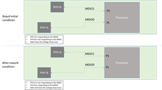
    The PHY A is an IC which is responding to the MDIO and is replaced with IC B which is not responding.

    Now we see that PHY B is responding, and PHY A is not responding.

    Question still remains, why is the MDIO voltage is dipping from 1.8V to 1.1V when the IC is active?

    Please let me know if you have any further debug points?

    Thanks & Regards,

    Nanjunda

  • Hi Nanjunda,

    Originally on your board there was PHY A which was responding to MDIO (does this mean register access was okay?). PHY A is replaced with PHY B and it does not respond to MDIO. Suddenly PHY B responds to MDIO but when it is replace with PHY A again, PHY A no longer responds?

    Were these replaced on the same board?

    Regards,

    Alvaro

  • Hi Alvaro,

    Yes, the PHYs are replaced on the same board.

    We have 2 PHYs connected to the Zynq FPGA. 1 each is connected to the PL section (FPGA) and other on the PS section(processor). 
    We see common issue on both the PHY's is the voltage on MDIO pin is dropping from 1.8V to 1.1V once the Clock input is provided to the Ethernet PHYs.

    I hope you can understand from the above image, we have interchanged the PHY-A to PHY-B positions on the board,

    Can we please get answers, why the voltage is dipping on the PHY? When PHY is not active (clock input is not given) the MDIO voltage is not dipping.

    Thanks & Regards,

    Nanjunda M

  • Hi Nanjunda,

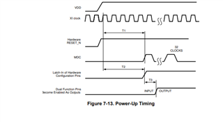
    What is the VDDIO voltage of the processor? Also, when you say provided the Clock input to the PHYs, is the rest of the board powered on? I understand we've already discussed the Power up timing but I want to be sure that it is still being followed, the clock should be present before the device receives power.

    once the Clock input is provided to the Ethernet PHY

    The DP83867ERGZ-R-EVM schematic files can be found in the link. Register access is available on that board, could you try comparing to your schematic? 

    Regards,

    Alvaro

  • Hi Alvaro,

    Thanks for the inputs.

    We tried the above condition with external clock source to the PHY, which will be present before the board is powered ON.

    We observed same behavior as before. The MDIO is dipping to 1.1V and there is no response on the MDIO.

    We are driving the PHY with 1.8V VDDIO voltage as shown in the schematics attached with post before.

    Please let us know how we can proceed further.

    Thanks & Regards,

    Nanjunda M

  • Hi Nanjunda,

    Something is missing here. What is the IO voltage of the Processor? Have you tried using the DP83867EVM and a MSP430 Launchpad to see how to read/write registers? With the launchpad connected to the EVM, USB-2-MDIO can be used to read registers from your PC.

    Please provide the following scope shots

    Shot 1:

    • All Power Supplies at power up
      • VDDIO
      • AVDD2V5
      • AVDD1V0
      • XI

    Shot 2:

    • At power up
      • VDDIO
      • RESET
      • MDC
      • MDIO
        • I want to see the transition from 1.8 to 1.1

    Regards,

    Alvaro