This thread has been locked.

If you have a related question, please click the "Ask a related question" button in the top right corner. The newly created question will be automatically linked to this question.

DP83825I: DP83825IRMQR query regarding EMI improvement

Part Number: DP83825I
Other Parts Discussed in Thread: DP83825EVM
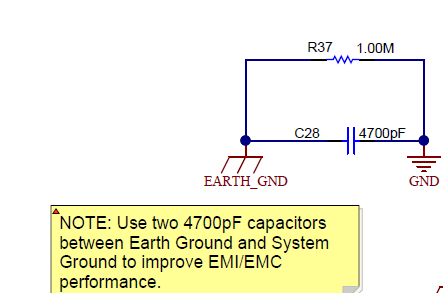
  • In the evk of DP83825IRMQR, its recommended to use 2 4700pf caps. Not able to understand single 4700pf with 1M cap can itself help EMI. Why 2 are recommended?
  • Also, how this network is helping to improve EMI.
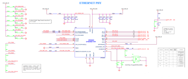
  • Share the EVK BOM.
  • attaching image below

  • Hi SM Kalim,

    The ground circuit pictured provides a better return path for any EMI noise.

    We are aware that the DP83825EVM's User Guide needs to be updated, the new revision will included the BOM. However, the design files for the EVM are on the product page and I was able to generate the BOM from them. Please find attached.

    HSDC045A(001)_BOM.xls

    Regards,

    Alvaro

  • Hi Alvaro,

    Thank you for the prompt response!

    Did you mean by adding 2 sets of RC network would provide better return path for EMI, Smooth transition wont be possible with single network? 

    Also can i go with 1M & 1000pf CAP(2KV) value to create the isolation between Chasis and Digital gnd?

  • Hi SM Kalim,

    I believe I understand your question now. There is no need for two RC ground Networks. I glossed over your first bullet and the note in the figure you provided. 

    You are correct, it is possible with a single RC network.

    Regards,

    Alvaro

  • Hi Alvaro,

     can i go with 1M & 1000pf CAP(2KV) value to create the isolation between Chasis and Digital gnd? I beleive both the logic would work same if i use 1M with 1000pf or 1M with 4700pf.

  • Hi SM Kalim, 

    I believe the 1000pF cap should be okay. If needed, this value can be tuned later when testing. I want to apologize for the confusion in my previous reply.

    We do recommend placing two of these RC circuits between the Earth Ground and Board Ground. 

    Screen shot taken from SNLA387, added the red line to show where the circuit should be.

    Regards,

    Alvaro

  • Hi Alvaro,

    In the EVK i could see a logic and unable to understand, please guide me

    There is a 33E resistor present between MAC & PHY (TX D0-RX D0) , (TX D1 - RX D1) &  (CRS DV - TX EN). What is the significance of these resistor and what would happen if i keep no mount in my design.

  • Hi SM Kalim,

    The purpose of these resistors is to "loopback" the data received from the cable side. In your design you wouldn't connect these pins to each other, instead the TX & RX pins would be connected to a MAC.

    Regards,

    Alvaro

  • Hi Alvaro,

    Thank you for the feedback!

    If I replace 33E with 22E, that would also work. I am planning to do this for BOM optimization for my project.

    Please confirm the above.

  • Hi SM Kalim,

    You are planning on looping the signals back? Could I ask why you would want to do this? If connecting to a MAC there would be no need for these series resistors.

    Regards,

    Alvaro

  • Hi Alvaro,

    Apologies for confusion.

    I will connect the phy with MAC only, just for de-bugging purpose providing the  loopback option. I will keep the 22/33E as No mount.

  • Hi Kalim,

    Understood, good luck!

    Regards,

    Alvaro 

  • Hi Alvaro,

    Hope your doing great!

    We have finalized the boot strap pins configurations as per our design need, could you please check and let us know if any changes need to be made.

    Also, 2.2k resistor has been kept as NM for boot strap configuration.

    Attaching the images and NM denotes no mount component.

  • Hello,

    Alvaro is OoO and will respond upon his return tomorrow.

    Sincerely,

    Gerome

  • Hi Kalim,

    Apologies for the delay in response, thank you for your patience. The strap settings look good and match what you have provided in the table. I would recommend to include the 2.2 kΩ R1 for MDIO. The datasheet says it "can be added if needed" but I would include it on your board.

    Regards,

    Alvaro

  • Thank you, Alvaro, for the support.

    Please find below the queries:

    • Can you guide me regarding pin3 (INTR/PWRD#)? Can I connect this pin to the AP's GPIO and provide a pull-up as NM?
    • I will set the PHY to work in slave mode, so pin2 (50MHZOUT/LED2/S/RX_DV_EN) won't be connected to the AP's input; it will be floating. Additionally, I will connect the AP's pin (50MHZ O/P) to the XI pin of the PHY, as the G2 pin (ENET_REF_CLK) of the AP is output only.
    • Also, I checked the APP NOTE while implementing RMII, and it states that the PHY's 50MHz pin should be connected to the AP's input. However, in my case, this condition is not possible. Could you please guide me on what the PHY's behavior would be if the 50MHz pin is not connected to the AP?
    • Refer to the highlighted table for better understanding.
    • Please refer to the attached image below, and note that the previous comment has been implemented.

    APPLICATION PROCESSOR

  • Hi Kalim,

    I have looked over your questions and have responded to them below. Please let me know if I missed anything.

    Can you guide me regarding pin3 (INTR/PWRD#)? Can I connect this pin to the AP's GPIO and provide a pull-up as NM?

    Yes you can, if R396 is installed this will work as intended.

    I will set the PHY to work in slave mode, so pin2 (50MHZOUT/LED2/S/RX_DV_EN) won't be connected to the AP's input; it will be floating. Additionally, I will connect the AP's pin (50MHZ O/P) to the XI pin of the PHY, as the G2 pin (ENET_REF_CLK) of the AP is output only.
    Also, I checked the APP NOTE while implementing RMII, and it states that the PHY's 50MHz pin should be connected to the AP's input. However, in my case, this condition is not possible. Could you please guide me on what the PHY's behavior would be if the 50MHz pin is not connected to the AP?

    The AP is providing the 50 MHz clock signal to the XI pin of our PHY, this is okay Thumbsup. I understand your confusion and want to reiterate that the PHY can work with the 50 MHz clock provided by the AP. In RMII slave mode the MAC and PHY need to share the same clock, but there is a sentence hidden in Section 7.3.10 Reduced Media Independent Interface of the data sheet that says it is okay for the AP to provide the clock to the PHY.

    Regards,

    Alvaro

  • Hi Alvaro,

    Thankful to you for the support

    So if i keep the 50MHZ pin2 as floating not connecting with the APs so it wont affect phy functionality. in this case this pin of phy will act as GPIO.Please correct me if im mistaken.

    Kindly review the latest shared image in the previous response. Let me know if any corrections needed from your end.

    also can you brief your statement, "Yes you can, if R396 is installed this will work as intended."

  • Hi Kalim,

    With the PHY in RMII Slave mode, Pin 2 will act as LED_2 by default. The functions of LED_2 can be changed via Register 0x460.

    I will review the image and provide more detailed feedback before end of day Wednesday, Jan 3rd.

    Regards,

    Alvaro

  • Hi Alvaro,

    I will await your valuable feedback.

    Also, can you guide me on providing the load resistor in between XI & XO pins of PHY when mounting the 25MHz crystal?

    Generally, we provide this resistor for stability and to control the clock from the crystal. I have provided a 1M resistor, R510 NM. Do we really need this resistor?

    If yes, why hasn't it been mentioned in the datasheet?

    Also, in the absence of this resistor, will the crystal not work as intended?

  • Hi Kalim,

    The load resistor and capacitors vary per vendor model of your crystal. Section 8.2.1.1.2 of the data sheet mentions it and provides a link to another document that has more detail information. 

    As for the review of your image,

    I recommend including:

    • R396
      • To keep INTR/PWRD in a known high state
    • Initially in your picture and table, you wanted RMII Master and your schematic was matched
      • But if you want RMII Slave you need to
        • Add R497
        • Remove R498 

    Everything else looks good. 

    Regards,

    Alvaro

  • Hi Alvaro,

    Thank you for the feedback!

    Please give your inputs on the below query:

    • As per the selection document the driver level of a crystal should be of maximum 100uW( SECTION 3.9), but the selected crystal is of 300uW. Would you recommend to change the crystal which have 100uW DL? If yes suggest the part number. Attaching the datasheet of current used part for your reference.
    • Also, there is series resistor RS recommended to add in at X0 pin. Refer to same section 3.9. This series resistor is valid for all the TI phy's or only for DP83 series phy's. The calculation has been done and we are getting 358OHMS and since its not a standard we are planning to go with 360ohms 1% resistor.

    CRYSTAL PART NUMBER- CS32-F1010FM08-25.000M-TR

    LOAD CAPACITOR-18PF

  • Hi Kalim!

    As per the selection document the driver level of a crystal should be of maximum 100uW( SECTION 3.9), but the selected crystal is of 300uW. Would you recommend to change the crystal which have 100uW DL? If yes suggest the part number. Attaching the datasheet of current used part for your reference.

    The section talks about the maximum power output of the crystal, and how you should not exceed that max (e.g. if the max drive output is 100uW, don't consistently consume 150uW, it'll degrade the crystal). The drive level as low as 100uW is an example of a minimum requirement. If the crystal you chose is 300uW, that's even better! I checked the data sheet you provided and this crystal meets our specs listed in Table 112 of the DP83825 Data sheet.

    As for the RS value, 360 should be okay but I want to reiterate that this would be a better question for the Crystal Vendor.

    Regards,

    Alvaro