This thread has been locked.

If you have a related question, please click the "Ask a related question" button in the top right corner. The newly created question will be automatically linked to this question.

DS280DF810: Register settings of DS280DF810

Part Number: DS280DF810
Other Parts Discussed in Thread: DS280MB810

Hi 

We have question about register settings of DS280DF810 below,

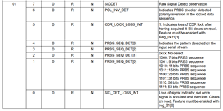
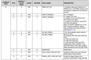
According to the Programmer's Guide of DS280DF810, we can see 7.43 Adjustable Output Swing Under Raw Mode.

When we changed REG_0x1A[7:6]=1 and REG_0x0D[0]=0 to REG_0x1A[7:6]=3 and REG_0x0D[0]=0 in case of Retimed mode(CDR Enabled),

we confirmed 25G communication error decreased.

Are these register settings effective for Retimed mode(CDR Enabled) not Raw mode ?

Does these registers change the bandwidth or something other than changing the amplitude?

And 

When we use Raw mode for 1G communication, could you please let us know if there are any registers that we should be careful about?

Thanks 

Kenji Mizobuchi

  • Hi Mizobuchi-san,

    Adjusting REG_0x1A[7:6] from 1 to 3 increases the bias current to several functional blocks in the retimer.  One impact of this is that retimer output VOD will increase.  I believe this is the impact you were intending to achieve.  Typically for retimed data, we typically recommend adjusting the output VOD through adjusting the FIR main cursor (see section 7.11).  Have you tried doing this instead of adjusting REG_0x1A[7:6] and if so, does this also improve your 25G performance?

    Are these register settings effective for Retimed mode(CDR Enabled) not Raw mode ?

    These register settings will have an impact in retimed mode, but typically we recommend adjusting VOD through FIR main cursor in retimed mode.

    When we use Raw mode for 1G communication, could you please let us know if there are any registers that we should be careful about?

    The following thoughts come to mind:

    • In RAW mode, you may need to manually adjust CTLE since retimer adaptation will not work.  However, it's also worth noting that the CTLE curve may not change much at 1G nyquist rate (625 MHz).
    • In RAW mode, FIR main cursor is not effective for changing VOD.  You are limited to adjusting VOD via Reg_0x1A[7:6].  Please keep in mind that adjusting Reg_0x1A impacts other function blocks and also impacts device power consumption.

    Thanks,

    Drew

  • Hi Drew-san

    Have you tried doing this instead of adjusting REG_0x1A[7:6] and if so, does this also improve your 25G performance?

    Yes,  but 25G performance improved when changing from main cursor +10 to main cursor +5 unexpectedly.

    About manual adjust CTLE, it is possible to increase CTLE boost gain for DS280DF810.

    But is it possible to decrease CTLE boost gain more than 9.2dB for DS280DF810 ?

    In the datasheet, it seems that minimum CTLE boost gain is 9.2dB.

    Thanks

    Kenji Mizobuchi

  • Hi Mizobuchi-san,

    Main cursor of +5 is lower than we often see for 25G amplitude.  Is the signal being sent to a module, or to an ASIC?

    Unfortunately, the DS280DF810 does not have a CTLE bypass stage.  There is not a direct way to lower minimum CTLE boost.  Setting a lower RPH level (REG_0x1A[7:6}) might lower CTLE boost, but may also impact other impacts of device performance.

    You could also try adjusting the EQ gain and VGA gain settings (section 7.32).  They apply broadband gain, so they are not expected to lower CTLE boost, but they might still be worth trying.

    Thanks,

    Drew

  • Hi Drew-san

    We have to use not only 25G but also 1G for DS280DF810.

    We understand  that bypass mode is needed to use for 1G.

    But  we found that there are some fragment packet errors not CRC error when we use our setting for 1G bypass mode.

    When we use your repeater DS280MB810, there are no error.

    Our setting for bypass mode is below, could you let us know if the settings are not appropriate for bypass mode ?

    1G bypass

    //setting channel Reg.

    address  value

    0xfc 0x01     

    0xff 0x03      

    0x00 0x04     

    0x0a 0x0c     

    0x2f 0x00     

    0x3d 0x0a    

    //ch 6/4/2/0 bypass CDR

    0xff 0x01     

    0xfc 0x55    

    0x0a 0x00    

    0x31 0x00    

    0x1E 0x00    

    0x2D 0x00    

    0x03 0x00    

    0x8E 0x01    

    0x13 0x20    

    //CH 7/5/3/1 power down driver,disable SD, PFD

    0xff 0x01     

    0xfc 0xaa    

    0x15 0x18    

    0x1e 0xec    

    0x14 0x44    

    0x13 0xF0    

    Thanks,

    K.Mizobuchi

  • Hi Mizobuchi-san,

    Reviewing your sequence, I see several cases where you are modifying register settings that I do not think you are intending to modify.

    Please keep in mind that many of the programming sequences in our programming guide include a write mask.  This mask indicates which bits should be modified for a given register write.  Typically this is handled through a read-modify-write (RMW) sequence.  Please see programming guide section 3.1.1 for more information on this.

    Reviewing your register writes, I've made a couple changes based on settings that I don't think you are intending to modify.  Please review these and confirm they are consistent with your intention.  I've highlighted register writes that I think should be modified in orange and my suggested writes in green.

    //setting channel Reg.

    address  value

    0xfc 0x01     

    0xff 0x03      

    0x00 0x04     

    0x0a 0x0c     

    0x2f 0x00     // In addition to setting rate, this disables PPM check

    0x2f 0x04

    0x3d 0x0a    

    //ch 6/4/2/0 bypass CDR

    0xff 0x01     

    0xfc 0x55    

    0x0a 0x00    // I would recommend holding CDR in reset until you're done modifying channel settings.  Suggestion is to move it to the end

    0x31 0x00    

    0x1E 0x00    // In addition to selecting raw mode, this enables DFE and disables PFD frequency detector

    0x1E 0x09 

    0x2D 0x00    // Modifies reserved bits.  Also, this does not override EQ control.  Assuming intention was to override EQ, see below.

    0x2D 0x38

    0x03 0x00    

    0x8E 0x01    

    0x13 0x20    // In addition to enabling EQ_HI_GAIN, this disables DC offset compensation and selects a test mode for the peak detector

    0x13 0xB0

    0x0a 0x00

    //CH 7/5/3/1 power down driver,disable SD, PFD

    0xff 0x01     

    0xfc 0xaa    

    0x15 0x18    

    0x1e 0xec    

    0x14 0x44    

    0x13 0xF0

    Can you try these modified settings and let me know if this improves the issue you're observing?

    Thanks,
    Drew

  • Hi Drew-san

    Thank you for your checking.

    We will check our setting based on your advice.

    Thanks 

    K.Mizobuchi

  • Hi Mizobuchi-san,

    Thank you for testing these settings.

    Looking forward to your update.

    Thanks,

    Drew

  • Hi Drew-san

    We checked our setting base on your advice.

    We confirmed that 0x2f 0x04 PPM check is effective for reducing errors.

    But we are not sure that PPM check function is for CDR mode.

    So, we do not think that bypass mode has anything to do with PPM check. Why ?

    Thanks,

    K.Mizobuchi

  • Hi Mizobuchi-san,

    The PPM check function is one of the first gating items to achieve CDR lock.

    With PPM check disabled, my hypothesis is that the retimer either attempts to get CDR lock to the 1G data, or momentarily gets false lock to the data.  If CDR lock is achieved, this would interrupt the data flow from the retimer as it switches from CDR bypass to retimed data signal chain.

    You can check if the retimer is momentarily getting CDR lock with PPM check disabled by observing the CDR_LOCK_LOSS_INT bit, ch_reg_0x01[5].  Please enable this loss indicator by settings ch_reg_0x31[1].

    Thanks,

    Drew

  • Hi Drew-san

    Thank you for your information.

    One question,

    In case of bypass mode for 1G

    Which is correct operation CDR_LOCK_LOSS_INT bit, ch_reg_0x01[5] =0 or CDR_LOCK_LOSS_INT bit, ch_reg_0x01[5] =1 ?

    Best Regards,

    Kenji Mizobuchi

  • Hi Mizobuchi-san,

    For CDR bypass mode, I would expect CDR_LOCK_LOSS_INT, ch_reg_0x01[5] = 0 since I would not expect the retimer to get CDR lock.

    Thanks,

    Drew

  • Hi Drew-san

    Thank you for your information about CDR_LOCK_LOSS_INT, ch_reg_0x01[5].

    We checked CDR_LOCK_LOSS_INT, ch_reg_0x01[5]  in case of 1G CDR bypass mode. The value was 0.

    As the detail of our problems,

    The re-timer is transmitting 1G using bypass mode(Port A).

    If the adjacent port outside the re-timer(Port B) is transmitting 1G, Port A will not have errors. 

    However, when transmitting 10G or 25G, errors will occur.

    This phenomenon looks like crosstalk  from adjacent port, but If using repeater, this phenomenon will not occur.

    We are conducting a cause analysis. 

    We use bypass mode of re-timer for 1G, but we suspect that CDR function is actually involved.

    Does CDR have no effect at all in bypass mode?

    Thanks,

    K. Mizobuchi

  • Hi Mizobuchi-san,

    Might it be possible to share a block diagram so I can better understand your issue?  It's not clear to me if the retimer is in the signal chain for both Port A and Port B in your example.

    Also, are these errors separate from the PPM check fix, or are these errors related?

    Thanks,

    Drew