Hii Ti masters,
I have designed my own display driver board using TFP401PZP TMDS DVI receiver/deserializer (from Mouser Electronics) which is connected to a 24bit parallel RGB 7 inch capacitive touch display of resolution 800x480.
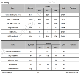
Display Datasheet: https://www.dwin-global.com/uploads/LCD-DATASHEET-LN80480T070IB3098.pdf
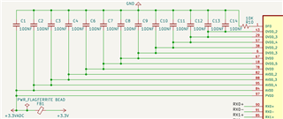
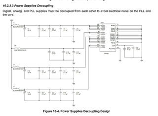
The power distribution is perfectly done to all segments. The driver board is designed on 2 layered PCB(Back layer is dedicated to only ground plane).
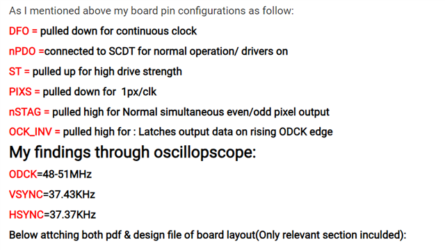
According to IC datasheet I've also set the pin parameters in following manner:
DFO = L
nPDO = H ,connected to pin 8 via 0ohm.
ST = H
PIXS = L , 1px/clk
nSTAG = H
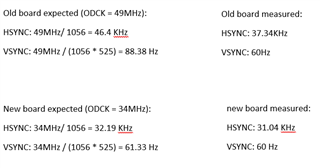
OCK_INV = H
Also set the EDID to external eeprom with 800x480 Resolution.
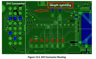
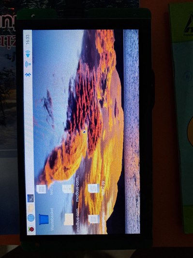
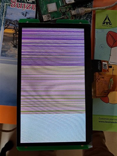
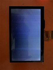
But at the output I'm getting distorted video(Ghost screen/Pixel mismatched)greenish horizontal lines.I've also shared the video output screen and Circuit board with schematic.
Links:https://imgur.com/a/pT2oVtv
Schematic below:
What might be the reason or what are the issues generally for this undesired video output?
Any help will be greatly appreciated.
Thanks & Regards
Arijit