Part Number: TUSB2E11
Hi Team,
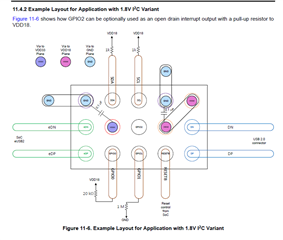
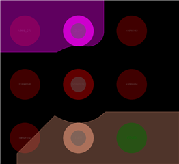
Could you please advise if we could place VIA for VDD33 and VDD18 just under the PIN? Or it is recommended to place a short trace to avoid the ball overlapping with VIA?
From DS, seems like VIA just be placed under the PIN. No concern for SMT? Thanks.

Best regards,
Terry


