This thread has been locked.

If you have a related question, please click the "Ask a related question" button in the top right corner. The newly created question will be automatically linked to this question.

SN65DSI86: SN65DSI86 MIPI Dual DSI interface 2@1920x1080 not working

Part Number: SN65DSI86

We have a Xilinx Artix-7 FPGA  design that produces two 1920 x 1080 MIPI video streams. Each stream is routed through a Meticom MC20902 chip before going to the SN65DSI86 chip. We are using the TI spreadsheet to generate register settings for the SN65DSI86 and I've verified that the timing values in the registers are correct. We can see 3840x1080 Display Port video out of the SN65DSI86 on the external monitor when we enable the SN65DSI86 test pattern. However, we are unable to successfully transfer DSI video through the SN65DSI86. We are only operating in single channel mode until we get a functional DSI interface. The MIPI stream as been modeled, checked and appears to be in compliance with the SN65DSI86 datasheet, but we have struggled with this device for weeks without making progress. We are operating the MIPI interface with a Xilinx D-PHY IP core driven by a custom DSI interface containing provisions to synchronize the DSI to a video frame sync input.  Is there a HDL behavioral model available to assist in determining what might be offending the SN65DSI86 DSI interface? Also, could you please direct us to a FAE operating out of the the San Diego region for assistant? Any other suggestions that might assist would be appreciated.

  • Hey Augusto,

    If possible can you send a schematic so I can have a look at that? Additionally, are you able to get the color bar to output?

  • Hello Vishesh,


    Yes, we are able to produce the color bars on the display, I have uploaded the pertinent schematic sheets.

  • Hey Augusto, 

    Looks like you are using REFCLK is that correct? Additionally, please include the .22uF capacitor on the EN pin. The schematic doesn't have any major issue so that should be ok.

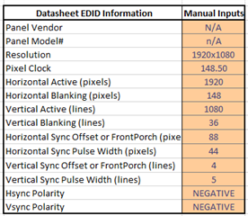
    If the color bar works and the DSI signal doesn't; then the issue lies in either the DSI signal or the register configuration. Can you send the filled out spreadsheet of you register values, and the panel spec? I will try to verify the registers. Can you have a look at the DSI signal and confirm that the video timings are correct?

    Also have a look at the error registers and see what the issue is. This is the guide: https://e2e.ti.com/support/interface-group/interface/f/interface-forum/945403/faq-sn65dsi86-sn65dsi86-black-screen-debugging-guide?tisearch=e2e-sitesearch&keymatch=sn65dsi86#

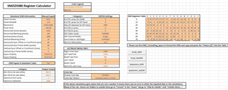
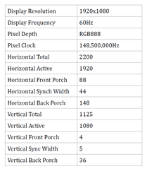
  • Yes, we are using REFCLK. Attached is a spreadsheet containing the register settings. The display requirements are also cited below.

    TI Support Bridge chip v1.xlsx

  • Hey I calculated the register values using the spreadsheet and our tool has different values. Try using the ones in this file:

    SN65DSI86_PANEL_VIDEOREGISTER_CALC_Augusto.xlsm

  • Hey,

    I'm closing this thread due to inactivity.

  • Hi Vishesh,


    We have incorporated the feedback from the updated spreadsheet you provided, but it still has not resolved our issue. We consistently receive:
    LOSS_OF_DP_SYNC_LOCK_ERR errors. What is the root cause of this error bit getting asserted?

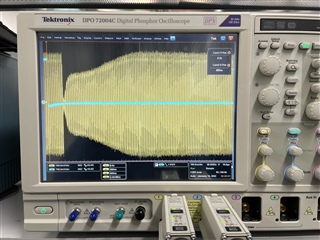
    Also, we discovered that the FPGA MIPI high speed clock amplitude was drooping while switching from low power to high speed mode. What would be the effect of this clock amplitude droop on the  SN65DSI86? I'm attaching a scope screen shot of a low power data line going low and it's subsequent affect on the high speed MIPI clock.

  • We consistently receive:
    LOSS_OF_DP_SYNC_LOCK_ERR errors. What is the root cause of this error bit getting asserted?

    The root cause is that the timing of the DSI and DP is mismatched:

    Can you send a dump of registers 0xF0 - 0xF8?

    What would be the effect of this clock amplitude droop on the  SN65DSI86?

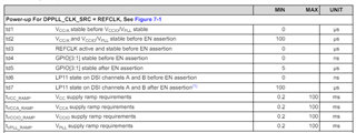
    This depends on when this happens. What is required is that the startup and power off procedure follow tables 8.4.2 and 8.4.3 respectively. and HS clock must be stable when the data is being transmitted.

  • 0xF0 - 0xF8 all read 0x00 except for 0xF6 = 0x40, LOSS_OF_DP_SYNC_LOCK_ERR

  • Hmm yeah it seems that the sync timings are not lining up.

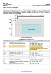
    Can you have a look at this and verify it is filled in properly for your system? I set the output type to RGB666 instead if RGB888 in the previous file. This is possibly why there are timing issues. 

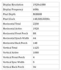
  • I had adjusted for the RGB666 to RGB888. Our timing is based on this:


  • Hmmm, can you confirm the DSI timings? From the looks of it the registers and ASSR are setup correctly for your panel, and this can be seen with the color bar. Meaning that the issue is stemming from the DSI inputs.

    Seeing as there is no PLL unlock it also means that the clock and speed of transmission is also ok. I think the best bet is to have a look at the DSI data and verify the line times, and then try swapping out the chip to see if that was the issue. It seems that you have everything set up correctly. 

  • Hi Vishesh,

    Is there a min and max time requirement for the low power state (LP-11) that must be observed for proper SN65DSI86 operation?

  • We are placing the MIPI lanes into the low power state once at the end of every frame. Would there be a min and max time requirement for the low power state under those circumstances? We've had some success in getting single channel video through the link. However, I suspect the duration of the low power period may be stalling our video link.

  • Why are you placing the MIPI lanes in a low power state after every frame? This isn't necessary

  • This only applies for burst mode. Are you in bust mode or non-burst?

    From my understanding this a non-bust continuous video stream, and disabling and re-enabling the lane may be the root cause of the issue.

    Can you try keeping all lanes active?

  • We are using non-burst. This is interesting new information. Thank you. I will modify the design to explore this option.

  • ok, keep me updated

  • I perform test that eliminated the low power period at the end of the frame, but unfortunately I was unable to transfer video in that mode. The bridge appears to become completely unresponsive without the low power period at the end of the frame. 

  • Hmm ok, can you send a dump of the error register 0xF0 to 0xF8

  • Also does the color bar still work?

  • The color bar still works. We are able to get video when we configure the chip for single channel and are using low power mode (all error registers are 0x00). When we disable low power mode (still single channel) then bit 1 in register 0xF6 get set (DPTL_UNEXPECTED_HSYNC_ERR) and we have no video output from the SN65DSI86 chip. When we enable low power mode and run in dual channel mode, then bit 6 in register 0xF6 gets set (LOSS_OF_DP_SYNC_LOCK_ERR) and we have no video output from the SN65DSI86 chip. Please let me know if you want me to get you errors in any other configuration. Augusto is on vacation for the rest of the week but he has a variety of FPGA builds that I can run for different experiments. The one experiment we can't run is burst mode though; the FPGA MIPI module we're currently using does not support that mode.

  • Hey Theresa,

    Are you able to verify the DSI timings? It seems that the issue is a configuration issue. 

    Are you able to got through the DSI register calculator and re-verify that nothings amiss? Are you able to test single input channel to single output channel?

    Use the same script you are using for the color bar and use that as the baseline for your DSI test script. Slightly modify this script and more forward with testing for signal channel input and single channel output. This has been a longstanding issue, and all errors point to a config/ DSI timing issue. 

    Also have a look at section 8.4.2 on the datasheet and make sure the power-on and power-off sequences are being met. The low power state is used for burst mode, so it should not be used for this testing.

    Is 0xF8 set to 0x01, this means that the semi-auto link training is successful.

  • Hi Vishesh,

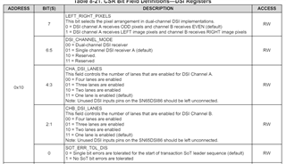
    I have verified I'm using the settings from the DSI register calculator spreadsheet and have verified the power-on sequence multiple times over the last year that we've been trying to get MIPI video to work. We are able to see single channel MIPI video from the FPGA output from the SN65DSI86 to the display. Link training is always successful. The only settings I change when switching to dual mode are register 0x10 (set to 0x80 instead of 0x20) and register 0x94 (set to 0xE0 instead of 0x20; probably not necessary to set single channel lower, but it works). When I restart with these register settings I get the LOSS OF DP SYNC LOCK error. The left and right side MIPI modules in the FPGA are identical and are configured identically.

    We have seen nothing in any documentation that says low power mode is only for burst mode. When we disable low power mode, we get no video at all (single channel video stops working). I didn't see any register settings for the mode; are there any registers I should change for this mode?

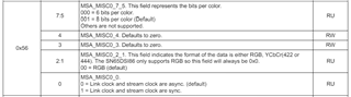
  • What are these pins set to? I cant see on the schematic sent. 

    the pins should be:

    GPIO1: 1

    GPIO2: 1

    GPIO3: 0

    GPIO4: 1

  • Are you able to got through the DSI register calculator and re-verify that nothings amiss? Are you able to test single input channel to single output channel?

    Are you able to have a look at the DSI signals?

  • By setting 0x10 to 0x80 you are also flipping the odd pixels from channel A and even pixels on channel B, to even pixels on channel A and odd pixels on channel B. Try setting 0x10 to 0x00. 

  • I thought the even/odd, left/right setting didn't matter in single channel mode. I do a power cycle when I switch between single and dual channel modes so the chip doesn't know what the previous setting was. I just changed setting 0x10 to 0xA0 in single channel mode but it didn't change anything (as expected). We need it to be left/right mode so 0x80 is the setting we need. I did try setting it to 0x00 to see what would happen but there was no change in behavior, so I changed it back to 0x80 for dual channel.

  • Hey Theresa,

    We are able to see single channel MIPI video from the FPGA output from the SN65DSI86 to the display.

    single channel works right, so now I'm looking at what would change between single and dual channel that would cause a failure. I wanted to see if switching which channel is even/ odd in dual mode would make a difference. 

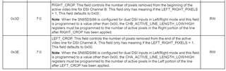
    Are either of these registers a non-zero value?

    If these are non-zero you will need to tune the line time by taking the crop into account.

    Also try synchronizing the stream clock and link clock to see if that helps.

  • when you change to dual mode do you calculate a new register setup as the DSI timings need to be changed as well. 

    single channel setup: SN65DSI86_PANEL_VIDEOREGISTER_CALC_Single_Theresa.xlsm

    dual-channel setup:SN65DSI86_PANEL_VIDEOREGISTER_CALC_Dual_Theresa.xlsm

  • Hi Vihesh,

    We are not using the crop registers, which are both zero. I can't use your spreadsheets as-is because we have an external 27MHz clock. In response to your question about what else changes when we switch to dual channel, I decided to generate a spreadsheet that compared the register settings in the files you provide above with the settings we're using in our code and the settings in the spreadsheets that we filled out (attached). Also, you had previously asked if we could look at MIPI signals. We have the ability to look at MIPI signals on an intermediate chip between the FPGA and the SN65DSI86, though the amount of video we can see on our scope at one time is limited. We have taken our board to another site to look at signals on a high speed scope and the signals and timing looked good. We have also switched GPIO 2 and 3 to outputs and looked at HSYNC and VSYNC on a scope, and those both looked good.

    Also, I tried even/odd, and the only difference was I stopped getting any errors (which appears to mean it's given up trying to interpret incoming video) even faster than normal.

    Theresa

    SN65DSI86 register comparison_Collins_2024-04-29.xlsx

  • Hey Theresa,

    Please clarify a few things, are you trying to display 1920x1080 video or 3840x1080 video?

    If the FPGA only produces 1920x1080 you cannot achieve 3840x1080 video. I have been working under the assumption you are trying to get the 1960x1080 monitor working, but it seems you script is for a video output of 3840x1080 as the timings dont align.

    My inputs:

    Differences:

  • Hi Vihesh,

    Our FPGA is generating two 1920x1080 video streams, so the SN65DSI86 chip is receiving 1920x1080 video on CHA and 1920x1080 video on CHB. We want the SN65DSI86 chip to put the two video streams together to output a single 3840x1080 video stream. When we only use a single channel then both input and output are 1920x1080, but when we use both channels we receive two 1920x1080 video streams and output a single 3840x1080 video stream.

  • Hey Theresa,

    You cannot put together two video streams of 1920x1080 to create a video stream of 3840x1080 using the DSI86. The color bar pattern you see on the 3840x1080 display is of the same aspect ratio not resolution so it appears to be at 3840x1080. The resolution going into the DSI86 must be the same resolution coming out of the DSI86. This is why single channel works with 1920x1080 but 3840x1080 does not. 

  • Hi Vishesh,


    For a one sink display port characteristics of 3840x1080 active at 60Hz with a pixel clock of 297.0MHz what is the required characteristics for MIPI DSI channel A and channel B in dual mode? The two source MIPI DSI ports (channels A and B) characteristics are currently 1920x1080 active at 60Hz with a pixel clock of 148.5MHz.. If I change the resolution of MIPI DSI channel A and B to 3840 x 1080 would the 148.5Mhz pixel clock still be acceptable? 

  • In the case where you are outputting 3480x1080 @ 60Hz from the FPGA, you would need to use a MIPI DSI splitter to divide the single stream into two streams. I am not sure what the output characteristics of the splitter would look like as TI does not offer such a part and thus is outside my area of expertise. The DSI clock can go up to 750MHz.

    The root cause of the issue isn't the resolution of the the input signals, but that you are using two different video inputs to drive one output. The DSI can only take information from one stream, but that single stream can be split up into channel A and channel B. If you are using two different streams to drive the DSI86 timing errors are expected. 

  • Im closing this thread due to inactivity

  • Hi Vishesh,

    We hadn't responded because we were so confused by your post. I think what you're saying is that if we want to output 3480x1080 video, then we need to input 3480x1080 video on channel A and input 3480x1080 video on channel B, which makes no sense at all. We also don't understand your reference to a splitter. I guess another way of interpreting your post is that we start with 3480x1080 video, feed it through a splitter to get 1920x1080 video on channel A and 1920x1080 video on channel B, then this chip will re-combine channel A and B to generate 3480x1080 video. This second scenario is the way we are trying to use it, but I think you said we can't use it this way. We would really appreciate it if you could clarify what the SN65DSI86 is expecting to get on channel A and on channel B in order for us to output 3480x1080 video from the SN54DSI86.

  • Hey Theresa,

    Sorry about my previous message being unclear. The DSI86 is not designed to take two independent streams and covert them into one single higher resolution stream. The reason channel A and channel B are implemented is so a single stream can be split up to allow for higher resolutions.

    For example, you are looking to output 3480x1080 @ 60Hz.

    H_Total = 4400

    V_Total = 1250

    Pixel_Clock = H_Total * V_Total * RR = 4400 * 1250 * 60 = 330000000 Hz

    Stream Rate = Pixel_Clock * 24bpp = 330,000,000 * 24 = 7,920,000,000 Hz


    DSI_CLK = 7920000000/ (2*4) = 990,000,000 Hz

    This minimum DSI_CLK is over the single channel maximum of 750MHz. And thus will not work with one channel. This is why channel B exists. The single 3480x1080 @60 Hz stream can be split into two streams by splitting the pixels by left/ right or odd/ even. This would effectively half the DSI_CLK frequency requirement to 495,000,000 Hz per channel allowing for the 3840x1080 stream to work with the DSI86. 

    The DSI86 may have two channels, but that is to be implemented for splitting one stream up and recombining it at the eDP outputs. The DSI86 is unable to take two separate streams and add them up, as the timings are impossible to line up.

  • Vishesh,

    Could you please explain this formula cited on page 31 of the data sheet?  This appears to contradict the previous post. Also, to clarify. we are not driving the bridge with "independent" streams. The video streams are driven from synchronized frame buffers. We have a 3840x1080 that is assembled with two 1920 X 1080 stream components that are synchronized. We are not attempting to combine unrelated video streams. Our left and right channels are synchronized / genlocked to each other.

  • Could you please explain this formula cited on page 31 of the data sheet?  This appears to contradict the previous post.

    This formula relates to the inputs of channel A and channel B. When a single stream is split into two, the Horizontal_Total is split into two as well either right/ left or odd/ even. This splitting of the horizontal pixel data results in two streams with the same timings divided by two. 

    We are not attempting to combine unrelated video streams. Our left and right channels are synchronized / genlocked to each other.

    Understood, sorry I misinterpreted.

    Are you able to send the register settings of the ref_clk working at 3840x1080? Additionally try to send two streams of 1980x540 and see if the timing issues are due to too many horizontal pixels.

  • The H_actives can be tuned via the right pixel start.

  • Hey, I'm closing this thread due to inactivity.

  • Hi Vishesh,


    I've had limited success using this device. We obtained single channel operation while operating the DSI/D-PHY and the bridge in a continuous video mode. However, with the A channel operational the B channels fails to operate in the dual channel mode even though the input data, resolution and timing are identical for both channels. In addition, we are trying to synchronize the MIPI stream to a vertical sync pulse and the low power state at the end of the frame appears to stall the bridge chip. Using this device has been a very disappointing development experience. I encourage TI to include HDL behavioral models and more working examples to support their customers using this device.  I have no further questions at the moment. I prefer to leave the thread open, but if you need to close it then close it, but my issues remains unresolved. If future questions arise I will post them as a new questions.

  • Hey Augusto,

    Sorry to hear that. I will look into finding/ creating a reference design and adding explanations and examples to avoid this in the future