This thread has been locked.

If you have a related question, please click the "Ask a related question" button in the top right corner. The newly created question will be automatically linked to this question.

TPD3S713A-Q1: CS pin

Part Number: TPD3S713A-Q1

Hello Team,

About the CS pin of TPD3S713A-Q1,

Is it dynamic or fixed compensation?

If dynamic,how to choose the DCDC feedback resistor R(FA)?

If fixed,I can choose the R(FA) according to the actual compensation voltage after test,then what's the function of CS pin?
  • Hi ,

    Thanks for reaching out.

    Eric has been assigned this thread and will be helping you with it.

    Thanks ,

    Shubha

  • Hi Ailing,

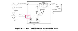
    The feedback scales with the load current.  For a larger load current, there is greater IR drop at the output, so we must increase the input voltage more to cancel out the losses.  This is described by figure 8-1 in the datasheet

    The equations for calculating each resistor can be found in section 8.3.2.1, where Rds_on = 73 mOhm (typical) and G_CS = 420 uA/A.  R_wire is dependent on your hardware design.

    You cannot adjust R_FA without also adjusting R_FB.  These two always need to add to the same value.  Otherwise, your zero-load output voltage will be incorrect.

    As an example, lets say I have a 5V converter with V_FB = 1 V.  I could setup a resistor divider of 4k+1k to satisfy V_FB.  Now let's split my 4k resistor into two series resistors.  The two values must always add to 4k to maintain the correct V_FB.  These become R_FA and R_FB.  The 1k is R_G.

    If I have a large output resistance (RDS_ON + Rwire), I need to increase my converter output a lot during heavy loading in order to maintain 5V at the system output.  If I only have a little output resistance, I only need to increase my converter output a little.  The combination of R_FA and R_FB control the amount of input compensation.  If I only need a little bit of increase in input voltage, most of my 4k comes from R_FB.  If I need more input compensation, I increase R_FA and decrease R_FB, keeping the sum of the two at 4k.

    Regards,
    Eric

  • Hello Eric,

    Thank you very much for your detail answer!

    The feedback scales with the load current.

    1.I still confused whether the CS is designed to adapt different USB cables or different USB devices?

    As an example, lets say I have a 5V converter with V_FB = 1 V

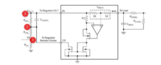
    2.The V_FB is the point1 or point2? If it is point1, as you said ,  R_FA+R_FB  is a constant value and R_G is also fixed, obviously the voltage  in point3 is always a fixed value.

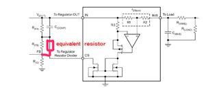
    3.In my opinion,I think the cs  is equivalent a resistor parallel to R_FB, and the equivalent value is changed with the load current.

  • Hi Ailing,

    1.I still confused whether the CS is designed to adapt different USB cables or different USB devices?

    It is designed to cancel out IR losses due to FET RDSON and trace resistance.  We do not identify any USB cable or device characteristics.  The ratio of I_CS to I_LOAD is fixed at 420 uA/A.

    2.The V_FB is the point1 or point2? If it is point1, as you said ,  R_FA+R_FB  is a constant value and R_G is also fixed, obviously the voltage  in point3 is always a fixed value.

    V_FB = Point 1.  Sorry for the confusion.

    3.In my opinion,I think the cs  is equivalent a resistor parallel to R_FB, and the equivalent value is changed with the load current.

    You have the right idea.  For your model, the equivalent resistor would be across both R_FB and R_G.  That is, the bottom of the resistor would be ground.

    More accurately, CS can be modeled as a dependent current source from Point 2 to GND, where I = 0.000420 * I_LOAD.  The current source points from Point 2 to GND.