Other Parts Discussed in Thread: TMDS64EVM, DP83867ERGZ-S-EVM, DP83869HM, DP83869EVM, DP83869
Hi Team,
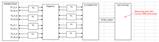
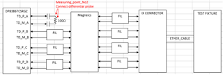
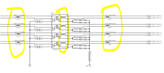
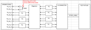
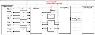
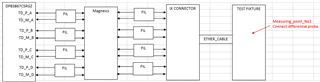
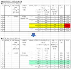
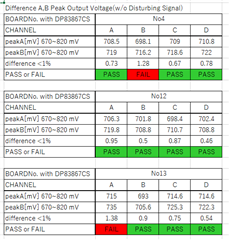
We are using DP83867CS on our development board,
An issue occurred during the 1000Base-T compliance test.
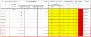
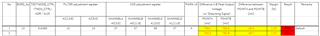
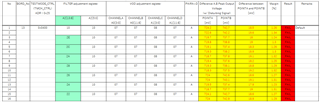
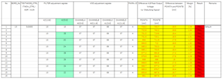
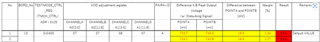
The test fails in the following section:
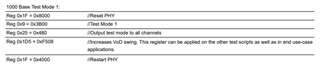
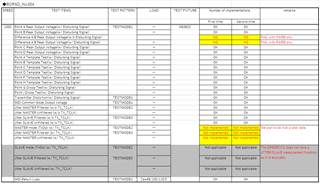
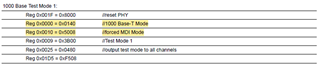
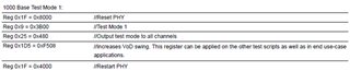
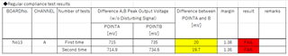
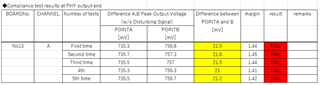
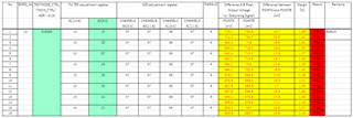
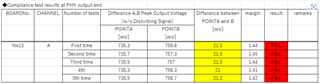
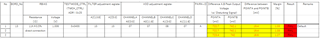
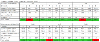
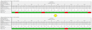
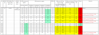
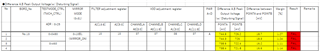
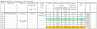
[1000 Base-T, difference A, B peak output voltage (w/o Disturbing Signal)]
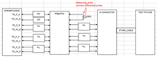
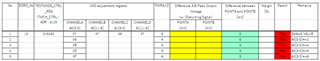
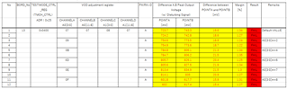
Please take a look at attached file for the details.
We would appreciate any advice regarding the results of the compliance test.
【Question1】
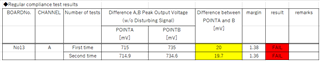
The above No.4_Board and No.12_Board and No.13_Board differ only in PHY parts.
From the above test results, I think there may be variations in port Difference A,B Peak Output Voltage depending on the component.
Could you please tell me how to improve the above?
【Question2】
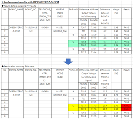
I checked a thread similar to this issue.
But I couldn't figure out how to improve it.
You can also see a thread about this issue in the E2E community, but it's a private communication and I don't understand the solution.
Could you please share your solution to resolve this issue?
<e2e>:e2e.ti.com/.../dp83867ir-10base-te-100base-tx-1000base-t-compliance-test
Best Regards,