This thread has been locked.

If you have a related question, please click the "Ask a related question" button in the top right corner. The newly created question will be automatically linked to this question.

TIC12400EVM-KIT: TIC12400EVM-KIT

Part Number: TIC12400EVM-KIT
Other Parts Discussed in Thread: TIC12400, , TXB0106, TIC12400-Q1

I am using TIC12400 EVM KIT , in technical document its is mentioned that App Center and TIC12400 GUI App software to be used. But i am not getting this software. what to do?  

  • Hi Amudha,

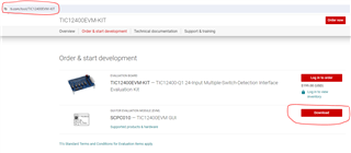
    The link to download the GUI can be found on the TIC12400EVM-KIT tool folder on ti.com. When you are on that page, scroll down and find the red Download button for the TIC12400EVM GUI.  (Link)

    Regards,

    Jonathan

  • i installed application but i didnt find the exact software(TIC12400EVM) ,what to do for that ?

  • What operating system are you using?  Is it Windows?  If so by default it should install inside a "Texas Instruments" sub folder in your program files directory. 

    C:\Program Files (x86)\Texas Instruments\TIC12400

    From the Windows Programs menu you should see a Texas Instruments folder and the "TIC12400 EVM" GUI run icon will be inside that if it has been installed.  You should also be able to see it listed in the Windows "Programs and Features" utility which is where you commonly uninstall programs.

    Can you see if you can find any indication it has been installed?  Or try to install it again and make note of the installation directory?

    Regards,

    Jonathan

  • How to observe output in TIC12400 EVM GUI application?

  • Iam facing to set the threshold  voltages in device settings how can i set the voltages ?

  • Hello Amudha,

    The TIC12400 Evaluation Module User's Guide (Link) gives very detailed information on how to configure the device settings, including the threshold voltages.  Section 5.4 of the User's Guide shows the Channel Configuration Page where you can set the comparator threshold levels for each channel.  Note, there is a "Simple View" and a "Detailed View" tab that allows you to make this configuration depending on your GUI preference.  There is also and "Advanced Settings" section you may want to use as well.

    Section 5.6 discusses the Real Time Status Tracker feature of the GUI where it will poll the status registers and display the status of all the enabled input channels. 

    You can also simply use the Register Map page to directly configure and read all device registers as discussed in section 5.9.

    Regards,

    Jonathan

  • How to observe output in TIC12400 EVM GUI application?

  • Amudha,

    Jonathan is out of office until next week, but I've notified another expert to see if they can help while he is out. Thanks for your patience.

    Regards,

    Eric Hackett 

  • Hi Amudha,

    Can you let me know how you wish to configure the device? For example, you can view the polling of the status registers and display the status of all the enabled input channels in the Real Time Status Tracker inside the GUI.

    Regards, Amy

  • How to connect TIC12400 WITH RH850?

  • Hi Amudha,

    The TIC12400EVM sold by TI uses a TI MSP430 MCU. 

    If you would like us to review your schematics, feel free to provide them here.

    Regards, Amy

  • which registers are need set read a switch status from

    TIC12400

  • How to read data from TIC12400?

  • Hi Amudha,

    How to connect TIC12400 WITH RH850?

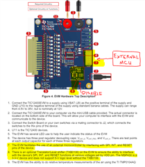
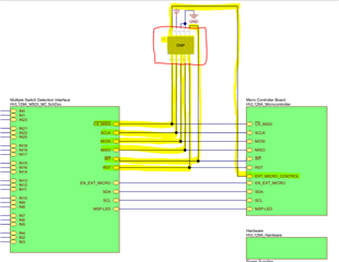
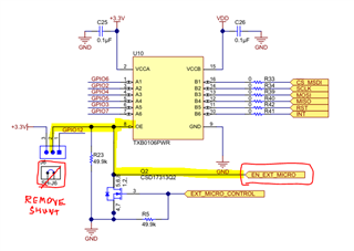
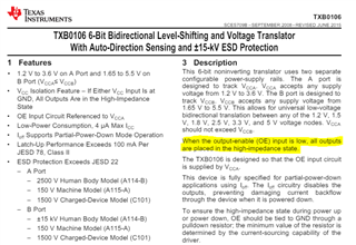
    You can connect an external MCU such as the RH850 to the TIC12400 EVM through Header J3.  You will need to disable the TXB0106 Level Shifter to isolate the SPI signal from the on-board MSP430 MCU and the TIC12400.  This can be done by removing the shunt on header J6 and either connecting pin 2 of J6 to GND, or connecting pin 10 of header J3 to GND.  This will set the Output Enable (OE) pin of the TXB0106 to a Low value and place the outputs to a high-impedance state preventing the MSP430 from interfering with the signals provided from the external MCU connected to J3.

    which registers are need set read a switch status from

    TIC1240

    How to read data from TIC12400?

    The TIC12400 Evaluation Module User's Guide (Link) provides a detailed overview of all the EVM hardware and GUI settings with step-by-step instructions on how to use the GUI to configure and read data from the TIC12400.

    The Steps to Configure TIC12400-Q1 Multiple Switch Detection Interface (MSDI) Application Report (Link) provides a detailed overview and steps needed to configure the TIC12400 and read the status results.

    After you have configured the device and set the TRIGGER bit to "1", you can read the INT_STAT_COMP register (0x05) to see the status of any enabled inputs that use the Comparator.  Or you can read the IN_STAT_ADC0 (0x06) and IN_STAT_ADC1 (0x07) registers to see the status of any enabled inputs that use the ADC.  The raw ADC codes for any enabled inputs that use the ADC  can be read from registers ANA_STAT0 - ANA_STAT12 registers 0x0A to 0x16.

    Regards,

    Jonathan

  • which registers are used to read data from TIC1200?

  • Amudha,

    What "data" do you want to read?  All device registers can be read to return their current value. 

    In my previous post, I provided the registers you need to read to return the status of the input channels.

    After you have configured the device and set the TRIGGER bit to "1", you can read the INT_STAT_COMP register (0x05) to see the status of any enabled inputs that use the Comparator.  Or you can read the IN_STAT_ADC0 (0x06) and IN_STAT_ADC1 (0x07) registers to see the status of any enabled inputs that use the ADC.  The raw ADC codes for any enabled inputs that use the ADC  can be read from registers ANA_STAT0 - ANA_STAT12 registers 0x0A to 0x16.

    Jonathan

  • Hi jonathan ,

    Please help Me with Write Data sequence and read Data sequence With A example .

    i am not Able to get it using Logic Analyser also the read and Write Cycle of The Register. 

    So Please let me Know how to read Device Id and what is is Data Pattern .

    Please also The The CPOL and  CPHA config for Ic . 

    If Possible Please Share the Sample Code for this.

  • Hi Amudha,

    I have provided an example in the other E2E post you created. (Link)  If you have additional questions, can we close one of these threads so we only have one open thread on this topic?

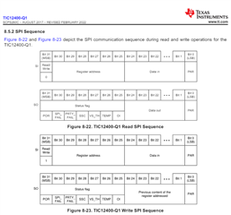
    The SPI protocol bit sequence is given in the datasheet in figures 8-22 and 8-23.  Note the most significant bit (or first bit transmitted after the chip select goes low) is the Read/Write Op Code bit.  It is followed by 6 bits of Address.  Note that the least significant address bit is not the least significant bit of the first byte.  The 24 bits of the data field are shifted by one bit due to the Parity Bit being the last bit in the sequence.  Therefore, you register address needs to be shifted to the left by one bit in the first byte of the transaction and you will need to write 0x02000000 in order to perform a Read of the Device ID register (address 0x01).

    I believe CPOL and CPOH should be 0.  Please verify your waveforms match the following I captured on a logic analyzer.

    Regards,

    Jonathan

  • Hi Jonathan,

    I am  Writing Data sequence and read Data sequence using GUI application

    i am not Able to get proper timing diagram of reading sequence, 

    i connected J1- open ,1 and 2 connected in J11 , 1 and 2 connected in  J12, 1 and 2 connected in J7 , 2 and 3 connected in J6 

    /resized-image/__size/320x240/__key/communityserver-discussions-components-files/138/pastedimage1715581643838v3.jpeg

    /resized-image/__size/320x240/__key/communityserver-discussions-components-files/138/pastedimage1715581643770v2.jpeg

    while reading the Device ID chip select pin behave like clock . The below link shows the timing diagram , please helps me to figure out the issue

    /resized-image/__size/320x240/__key/communityserver-discussions-components-files/138/pastedimage1715584001175v1.png

    Thanks

    Amudha

  • Hi Amudha,

    The images you inserted are a little too low resolution for me to see any detail.  But based on your description that the chip select signal is acting like a clock, I would suspect that you are getting some cross talk on the SPI signals causing problems with the TXB0106 Level shifter. 

    These level shifter IC's are Bidirectional and have an auto-direction sensing feature that makes them susceptible to noise which can cause the device channel to switch directions if it sees some noise on the "output" side which will cause it to think that it needs to switch directions in order to not block any bi-directional data.  

    By placing the logic analyzer probes in the middle of your data connection, we now have a source for reflections in the signals and cause problems with the auto-direction feature.  There are 0-ohm resistors on the signals that could be replaced with a larger value (i.e. 330 ohm, etc.) that would help dampen any signal reflections and improve the communication.  I don't know what value would be needed, or if this would prevent the issue all of the time, but I am pretty sure the issue is with the level shifter switching directions and interrupting the SPI communication.

    I don't currently have any other recommendations on how to bypass or stabilize the TXB0106 and reliably capture the SPI communication between the MSP430 and the TIC12400-Q1 on the EVM when using the GUI.  To capture the Device ID Read waveform I previously shared, I was using an external MCU for the SPI and did not have the TXB0106 enabled.

    If there are any specific register read/write waveforms you are interested in, I could try to help capture those for you.  If you are still unclear on the protocol, I can also try to simplify that with additional examples as well.

    Regards,

    Jonathan

  • Hi Jonathan,

    we are try to read device id from command reg  01h.

    My Data is like 0x02, 0x00, 0x00, 0x00

    and from the Device We are Receiving 0xE1, 0x00, 0x41.

    So i am considering the data is shifted by one bit so it is only 0x20 if confirm is it correct.

    also read patten says 0th bit is Parity bit and it should be zero so why i am getting this as 1 .

    Please Help  with some sample code .

    Regards

    Amudha 

  • Hi Amudha,

    The data you are sending on the MOSI signal of 0x02, 0x00, 0x00, 0x00 is correct for a Read of the Device Register 0x01.  However, the received data on the MISO signal of 0xE1, 0x00, 0x41 is completely incorrect.  I've added this logic analyzer plot of a Device ID Read in an earlier post, but you can see what the waveforms should look like.  Your response data should be <status byte value>, 0x00, 0x00, 0x40.  Note the first byte returned is the status byte, so it is unknown, but the last 3 bytes contain the register value being returned.

    The device uses Odd Mode Parity, meaning that the total number of 1's in the SPI transaction should be an Odd number.  Therefore if the total of number of 1's in the SPI message without including the Parity Bit is an odd number, then the parity bit should be set to "0" to keep an odd number of 1's.

    However, if the number of 1's in the SPI message without including the Parity Bit is an Even number, then the parity bit should be set to "1" to make the total number of 1's and odd number.

    Therefore, sometimes the parity bit will be 1, and sometimes it will be 0.

    Are you making sure to disable the TXB0106 Level Shifter through the J6 header when you are trying to communicate from an external MCU?  If you don't disable this level shifter when using an external MCU, then it will cause communication problems.

    Regards,

    Jonathan

  • Hi Jonathan,

    As you said we have checked your above suggestions and , now We are able to read device id , with command 0x02, 0x00, 0x00, 0x00 .

    and we Get from IC , 0x00 ,0x00, 0x00 , 0x40.

    So in 2nd Setup we just try to read the INTP Status Reg Which fall on Add 0x02 , Here We Sending 0x04, 0x00, 0x00,0x00.

    After this the INTP Is Getting Clear and visible on Board with help of led, But at read we are getting Parity bit is One . And as Per parity bit logic It should be in odd number , So at our Command we Sending only 1 One In data so it is in odd number so here basically Parity should not fail  but then Also We are getting the Parity Error .  So Please Suggest The Data for This register or Give More Clarity on the Parity bits .

    Regards

    Amudha D

  • Hi Amhuda,

    I'm glad you are now able to read registers.  Your description of the data appears correct to me and I'm not sure based on that why you are seeing the parity error.  Can you try to read the INT_STAT register (0x02) multiple times to see if it gets cleared by the first read, or whether it remains set? 

    Are there any other bits getting set in the INT_STAT register?

    Can you also try to read other registers and make note of whether the parity bit is only getting set for certain registers, or for all registers and whether we can determine some sort of pattern or relationship between when it is getting set, or not set to help determine what the reason for it is?

    Are you able to write and read back a register to verify that is working properly?

    As long as you have the TXB0106 level shifter disabled, you should be able to use a logic analyzer as well.  Can you try to capture the SPI communication between your processor and the TIC12400-Q1?

    I'm also attaching a simple excel spreadsheet tool I have created to help encode and decode the MOSI data between the R/W, Address, Data, and Parity fields into the format required by SPI. It may be helpful to you for verifying the format of the data you are sending to the TIC12400 and whether the Parity bit should be a 1 or 0.

    .TIC12400-Q1 Register Value SPI Sequence Calculation Worksheet Rev A.xlsx

    Regards,

    Jonathan

  • Hi Jonathan,

    The problem i faced about the parity bit is resolved .

    Now i am trying to read the 10 switches based on input enable bits in IN_EN register (IN0-IN9).

    I configured the below registers

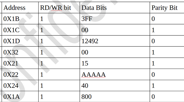
    ADDRESS=1A = IN_EN -  B60007FE (WR=1,PARITY=0,DATABITS=0003FF)

    ADDRESS=1C = CS_SEL - B8000001 (WR=1,PARITY=1,DATABITS=000000)

    ADDRESS=1D = WC_CFGO - BA000000 (WR=1,PARITY=0,DATABITS=000000)

    ADDRESS= 32 = MODE - E4000001 (WR=1,PARITY=1,DATABITS=000000)

    ADDRESS= 1A = CONFIG - B4000001  (WR=1,PARITY=1,DATABITS=000000)

    ADDRESS= 21 = THRES_COMP - C2000055 (WR=1,PARITY=1,DATABITS=00002A)

    ADDRESS= 22 = INT_EN_COMP1 - C4AAAAAA(WR=1,PARITY=0,DATABITS=555555)

    ADDRESS= 1A = CONFIG - B4001000 (WR=1,PARITY=0,DATABITS=000800)

    Reading registers are mentioned below

    ADDRESS= 02 = INT_STAT

    ADDRESS= 05 = IN_STAT_COMP

    After changing the SW0 - SW9 switch state, in result no change (INT_STAT = 00000001,IN_STAT_COMP = 00000001 registers) 

    Regards,

    Amudha.

  • Hi Amudha,

    ADDRESS=1A = IN_EN -  B60007FE (WR=1,PARITY=0,DATABITS=0003FF)

    The IN_EN register address is 1B.

    ADDRESS=1D = WC_CFGO - BA000000 (WR=1,PARITY=0,DATABITS=000000)

    You have set the wetting current levels to 0mA for all switches.  This is likely incorrect for use with the EVM unless you have provided an external voltage source to all the switches so that there is a path for current to flow.  The general operation of the device is that it will source some current out of the INx pin which will flow through the external switch resistance to GND.  This results in a voltage drop that can be detected by the Comparator or ADC based on Ohm's Law (V=I*R).  When the switch is Open, there will be a high resistance and the INx pin will have a voltage that is greater than the detection threshold.  But when the switch is closed, there will be a low resistance and the INx pin will have a voltage lower than the detection threshold.  When you set the wetting current level to 0mA, you will not be able to detect the difference between an open or closed switch without an external supply voltage connected to the switch.  I would suggest setting the wetting current levels to a non-zero level such as 2mA.

    ADDRESS= 22 = INT_EN_COMP1 - C4AAAAAA(WR=1,PARITY=0,DATABITS=555555)

    I see you want to have interrupts generated for on the INT pin, then you will also need to set the SSC_EN bit in the INT_EN_CFG_0 register (0x24:2 = 1).

    Regards,

    Jonathan

  • Hi Jonathan,

    As per the above configuration i have  enabling Sw0 - SW9 in comparator mode

    we read the registers 2h  INT_STAT Interrupt Status Register and 5h   IN_STAT_COMP Comparator Status Register

     but we cant get any value.

    Regards,

    Amudha

  • Hi Amudha,

    I think you overlooked the final suggestion in my last post. 

    I see you want to have interrupts generated for on the INT pin, then you will also need to set the SSC_EN bit in the INT_EN_CFG_0 register (0x24:2 = 1).

    When I load your register configuration into my EVM and also set the SSC_EN bit in register 0x24, then I see the SSC bit change in the INT_STAT register when I change a switch.  Hopefully this will work for you as well.

    Regards,

    Jonathan

  • Hi Jonathan,

    I have one about ADC reference voltage, in the given datasheet there nothing mentioned about ADC reference voltage can you tell me about the ADC reference voltage. And when i need to convert into 5v how is configured.

    Regards,

    Amudha

  • Hi Amudha,

    The ADC uses an internal reference and specifies the full scale range which is 0-6V for the INx channels.  The ADC can also be used to monitor the VS supply voltage and if enabled, there are two scales available that can be chosen from in the register configuration.  The first VS range is 0-9V, and the second is 0-30V.

    Therefore an INx pin voltage of 6V would return an ADC code of 1023.  When 5V is applied to the INx pin the ADC would return a code of approximately 853.

    5V / ( 6/1023) = 852.5

    Regards,

    Jonathan

  • Hi Jonathan,

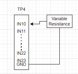
    1. I have to read the resistance using ADC channels. While connecting variable resistance in IN10 & IN11 pin the ADC maximum value reaches at 6250 ohms and IN12 - IN23 pin the ADC maximum value reaches at 10M Ohms, why that much different to reach maximum adc value? what is the maximum resistance value to achieve 1023?

    2. My Assumption, The Threshold in this IC is used to generate Interrupt. and let me know how to used those threshold in effective way?

  • Hi Amudha,

    Can you tell me the configuration you are using and how the resistance is connected in the circuit?  Perhaps a simple schematic diagram if that is easier?

    Are you using current source or sink mode?  What is the wetting current levels?  What is the VS supply pin voltage?

    The device works on Ohm's Law (V=I*R) and the ADC range is between 0V and 6V as measured on the INx pin.  Therefore I will need to know all the factors to understand your observations.

    Regards,

    Jonathan

  • Hi Jonathan,

    Configuration

    Enabling IN10-IN23 pins
    setting current source
    Wetting current as 1mA
    mode setting IN10-IN23 pins as ADC
    Threshold comparator (2V)
    ADC threshold config0- THRES1 - 150, THRES0 - 000 (DATA bits In Hex 0X025800)
    ADC threshold config1- THRES3 - 450, THRES2 - 300 (DATA bits In Hex 0x04C92C)
    ADC threshold config2- THRES5 - 750, THRES4 - 600 (DATA bits In Hex 0X0BBA58)
    ADC threshold config3- THRES7 - 850, THRES6 - 800 (DATA bits In Hex 0X0D8B20)
    ADC threshold config4- THRES9 - 950, THRES8 - 900 (DATA bits In Hex 0X0EDB84)
    ADC threshold map0- (DATA bits In Hex 0X0000)
    ADC threshold map1- (DATA bits In Hex 0X011000)
    ADC threshold map2- (DATA bits In Hex 0X0000D1)
    INT Enable Comparator1(0x22)- (DATA bits In Hex  0XAAAAAA)
    INT Enable Comparator2(0x23)- (DATA bits In Hex  0XAAAAAA)
    Global Interrupt Gen Reg(0x24)- (DATA bits In Hex  0X000040)
    ADC Interrupt enable gen reg0(0x25)- (DATA bits In Hex  0x222222)
    ADC Interrupt enable gen reg1(0x26)- (DATA bits In Hex  0XAAAAAA)
    ADC Interrupt enable gen reg2(0x27)- (DATA bits In Hex  0XAAAAAA)
    ADC Interrupt enable gen reg3(0x28)- (DATA bits In Hex  0X00AAAA)
    config trigger (0x1A)- (DATA bits In Hex  0X000800)


    VBAT -12V
    Vs - 11.8V

    Schematic

    My Assumption, The Threshold in this IC is used to generate Interrupt. and let me know how to used those threshold in effective way?

    Thanks 

    Amudha

  • Hi Amudha,

    Section 6 of the Steps to Configure TIC12400-Q1 Multiple Switch Detection Interface (MSDI) Application Report (Link) provides a detailed overview and steps needed to configure the TIC12400 inputs for use with Resistor coded switches using the ADC.  I would think this will address many of your questions.

    For your previous question about the max ADC code for a resistance value, the INx pin voltage should always be equal to the result of Ohm's law (V=I*R) when using current source mode.  If you are always sourcing 1mA of current, then you should get a max ADC code with 6K resistance.  If you are seeing a difference, then something else is the problem.

    Note the INx pin voltage is a little different when using current sink mode because the voltage drop from Ohm's Law is subtracted from the VS or Vbatt voltage connected to the high side of the switch.

    Note that the comparator and ADC threshold and interrupt configuration settings are independent.  Therefore if you are using the ADC, you do not need to set the Comparator settings for that channel.

    Note there are shared wetting current and ADC and Comparator threshold configuration settings that are shown in table 8-1 in the datasheet.  Each INx channel is not independently configurable.

    Generally speaking, you will need to determine an ADC code to assign to a the thresholds and then you will need to select the threshold that should be used to generate an interrupt.  When these are configured and enabled, an interrupt will be generated when the ADC value crosses the threshold.  Some inputs have multiple thresholds.

    Regards,

    Jonathan

  • Hi Jonathan,

    We need to read resistance 1 ohm to 300 ohm only. And if we are reading resistance each ohm, corresponding ADC value also need to change .

    Can you explain how it will be possible? 

  • Hi Amudha,

    When using the current source configuration where the resistance is placed between the INx pin and GND, it is as simple as Ohm's Law (V = I * R) where the INx pin voltage measured by the ADC is equal to the wetting current multiplied by the resistance.

    The ADC has a 0V to 6V range meaning that if the voltage on the INx pin exceeds 6V, the maximum ADC code of 1023 will be returned.  But if the voltage on the INx pin is between 0V and 6V, an ADC code between 0 and 1023 will be returned corresponding with the voltage.

    First you need to know the resolution or the voltage range for a single ADC code which is: 6V / 1023 = 5.865mV.  So this tells you that the voltage levels corresponding with the different resistor levels you are trying to detect must be greater than 5.865mV, or the same code will be returned for both resistance levels and you will be unable to detect the difference with the ADC.  Changing the wetting current level will result in a different voltage for the resistor, so larger wetting current levels results in larger voltage differences.  But you only have a 6V detection range, so we need to make sure the voltage at your largest resistance is less than 6V.

    If you used the 1mA wetting current level, you would get a voltage difference of approximately 1mV for each ohm of resistance.  This would only use 0V to 0.3V of your available ADC detection range and each ADC code would represent 5-6 ohms.  So this is probably too little.

    However the max wetting current level of 15mA, would give you about 15mV of voltage difference for each ohm of resistance which is approximately equal to 3 ADC codes.  The maximum resistance of 300 ohms would result in 4.5V at the INx pin which is less than 6V, so this is probably the best setting to use because it gives you the largest ADC code resolution because you also need to accommodate the various tolerance factors.

    Regards,

    Jonathan

  • However the max wetting current level of 15mA, would give you about 15mV of voltage difference for each ohm of resistance which is approximately equal to 3 ADC codes.  The maximum resistance of 300 ohms would result in 4.5V at the INx pin which is less than 6V, so this is probably the best setting to use because it gives you the largest ADC code resolution because you also need to accommodate the various tolerance factors.

    Hi Jonathan,

    Is this possible to detect the input state of the pin (example: High(+vcc) , Low(GND)) using the TIC12400

    Regards 

    Amudha

  • Hi Amudha,

    The ADC has a detection range of 0V to 6V.  If the voltage on the INx pin is greater than 6V, the ADC will saturate and return the maximum code of 1023.  But a unique code between 0 and 1023 for a voltage within the range of 0V to 6V.  This works out to be that each ADC code represents approximately 5.8mV.

    Regards,

    Jonathan

  • Hi Jonathan,

    Is this possible to detect the input state of the pin (example: High(+vcc) , Low(GND)) using the TIC12400

    Regards 

    Amudha

  • Hi Amudha,

    If you are using the Comparator, then the device will let you know whether the voltage is above the configured threshold (2V, 2.7V, 3V, or 4V). 

    If you are using the ADC, the device has a sampling range of 0V to 6V and you can either read the raw ADC code and calculate the voltage if it is within this range.  If the ADC code is the maximum value of 1023, then you can only determine the voltage is greater than or equal to 6V.  The ADC also has programmable thresholds that can be set to specific ADC code values.  The device can then generate interrupts when the voltage between readings change values that cross the configured threshold.

    Regards,

    Jonathan