Part Number: SN65DP159
Hi Forum,
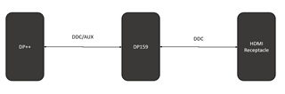
I am making this thread as a verification that I have routing pins 38 and 39 correctly on the SN65DP159RSBR IC. These pins are the SCL and SDA lines for interfacing with DP source. While updating the CCA that uses this IC, I needed to reroute the trace connected to these two signals. In the previous layout, these lines were routed as differential pairs with controlled impedance. Due to limited spacing after updating the CCA, I cannot route these as controlled impedance anymore but just as regular SE traces.
I did not find anything about needing to route these pins as controlled impedance in the SN65DP159RSBR datasheet. However, looking through the HDMI spec, I found that this I2C signal along with the sink I2C signal is to run DDC bus functions such as reading EDID info from the HDMI sink. The DDC bus shall be run at 100k or 400k, which is Standard mode and Fast mode I2C. Such speeds do not need controlled impedance, hence I rerouted the traces connected to pins 38/39 of SN65DP159RSBR as regular traces.
I would like to receive verification that this is the correct design choice or whether I made the wrong choice and need to change these signals to differential pairs. Please advice.
Thank you,
Lu Tan