This thread has been locked.

If you have a related question, please click the "Ask a related question" button in the top right corner. The newly created question will be automatically linked to this question.

SN65HVD09: Output differential load driving current capabilities at various temperature Reg

Part Number: SN65HVD09

Tool/software:

Dear team,

We are using SN65HVD09 RS422 driver in our device for communication, Please share the load driving current capability of the device at various temperature.

Kindly share the output RS422 load driving current (max) Vs Temperature graph(-40degC to +85degC) for our analysis. Without degradation of RS422 driver output differential voltage.

Thanks in advance

  • Ajith,

    We don't really have the data you are asking for.

    These devices are designed around the RS485 standard so we have some clues around what kind of loads they can drive. 

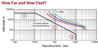
    From a capacitive sense vs frequency/data rate. They should be able to support around 20Mbps if you're okay with 5% jitter

    For region 2, it's based on the jitter/AC response. From a cabling perspective, generally we assume about 50pF per meter so this gives you a rough estimate on the capacitive loads RS 485 devices can drive.(dependent on frequency/datarate). So the capacitance it supports varies with the data rate at higher speeds over 100kbps.

    Region 1 looks at the DC response (DC resistance) so you can use this to approximate cable resistance as well. (maybe around 18ohms per 1000 Ft or close to 60 ohms at 1kM). So at 1 kM you will have an attenuation of about half your sent signal at the received side. (60 ohm total termination with 60 ohm series resistance). 

    Please share the load driving current capability of the device at various temperature.

    The device is capable of withstanding short circuits up to 260mA on a driver. (the e2e link you provided looks like this is actually limited to around 80mA likely due to the FETs getting saturated). Figure 14 of the datasheet already gives you an estimate of this. The left curve is at the lower temperature range (I suspect -40C) the middle curve is at room temp of around 25C and the right curve is likely at 85C. These tests are done with only 1 unit so the data isn't going to provide great statical detail. (Neglects process doping levels)

    Kindly share the output RS422 load driving current (max) Vs Temperature graph(-40degC to +85degC) for our analysis. Without degradation of RS422 driver output differential voltage.

    This type of analysis would require some kind of silicon aging analysis. This device is from 2008, we don't have the capability to look into the simulations for this device on a design level because of how old the database is (we likely can't find it). My guess is if you're asking for max load support then you're expecting to short the device over long periods of time, the failure rate in time could increase. This is a result of the metal traces heating up and cooling off a lot of time which could eventually cause them to break. The device has an internal thermal shut down of 165C so the metal is likely to heat up a bit before this kicks in (these thermal shut down parameters usually have a bit of tolerance to them as well.....) 

    -Bobby