Part Number: TCAN4551-Q1
Tool/software:
Hi, team,
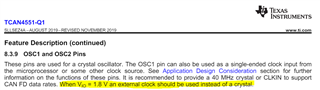
my customer encountered an issue when using TCAN4551, when power up and the VIO is 1.8V, but they find the clock don't work and the SCH, register configuration are as attachments. Could you help to analysis the issue and give some suggestions? Is there default configuration in TCAN4551 after power up? Is it necessary to write configuration to work properly? what should we do before the clock start?
#define OSI_LOG_TAG OSI_MAKE_LOG_TAG('M', 'Y', 'A', 'P')
#include "stdio.h"
#include "osi_log.h"
#include "hwregs.h"
#include "drv_spi.h"
#include "drv_names.h"
#include "hal_chip.h"

#include "TCAN4550.h"
#include "TCAN4x5x_Data_Structs.h"


volatile uint8_t TCAN_Int_Cnt = 0;					// A variable used to keep track of interrupts the MCAN Interrupt pin
extern drvSpiMaster_t *tcan455_spidrv;
extern void SPI_init(void);
extern void Canopen_CO_CANinterrupt(void);

void SPI_init(void)
{
	halPmuSetPowerLevel(HAL_POWER_SD, POWER_LEVEL_1800MV);
	halPmuSwitchPower(HAL_POWER_SD, true, true);


	halIomuxSetFunction(HAL_IOMUX_FUN_SPI_1_CLK_PAD_SDMMC1_DATA_3);		//CLK
	halIomuxSetFunction(HAL_IOMUX_FUN_SPI_1_CS_0_PAD_SDMMC1_DATA_4);	//CS0
	halIomuxSetFunction(HAL_IOMUX_FUN_SPI_1_DIO_0_PAD_SDMMC1_DATA_5);	//SDI
	halIomuxSetFunction(HAL_IOMUX_FUN_SPI_1_DI_1_PAD_SDMMC1_DATA_6);	//SDO

	halIomuxSetFunction(HAL_IOMUX_FUN_GPIO_0_PAD_GPIO_0);
	halIomuxSetFunction(HAL_IOMUX_FUN_GPIO_1_PAD_GPIO_1);
	halIomuxSetFunction(HAL_IOMUX_FUN_GPIO_44_PAD_CAMERA_RST_L);

	static drvGpioConfig_t gpiocfg_rst;
	gpiocfg_rst.mode = DRV_GPIO_OUTPUT;
	gpiocfg_rst.out_level = 0;
	drvGpio_t* pDrvGpio_rst = drvGpioOpen(44, &gpiocfg_rst, NULL, NULL);	//GPIO0
	if(NULL != pDrvGpio_rst)
	{
		OSI_LOGI(0,"OSI_LOGI drvGpioReconfig = %d",drvGpioReconfig(pDrvGpio_rst, &gpiocfg_rst));
	}
	bool level = drvGpioRead(pDrvGpio_rst);
	OSI_LOGI(0,"GPIO_rst 0= %d",level);

	drvGpioWrite(pDrvGpio_rst, 1);
	level = drvGpioRead(pDrvGpio_rst);
	OSI_LOGI(0,"GPIO_rst 1= %d",level);

	osiThreadSleep(10);
	drvGpioWrite(pDrvGpio_rst, 0);
	level = drvGpioRead(pDrvGpio_rst);
	OSI_LOGI(0,"GPIO_rst 0= %d",level);


	drvSpiConfig_t spiCfg = {0};
	spiCfg.name = DRV_NAME_SPI1;
	spiCfg.inputEn = true;
	spiCfg.framesize = 8;
	spiCfg.oe_delay = 0;
	spiCfg.baud = 2000000;
	spiCfg.cs_polarity0 = SPI_CS_ACTIVE_LOW;
	spiCfg.cs_polarity1 = SPI_CS_ACTIVE_LOW;
	spiCfg.cpol = SPI_CPOL_HIGH;
	spiCfg.cpha = SPI_CPHA_2Edge;
	spiCfg.input_sel = SPI_DI_1;
	spiCfg.transmode = SPI_DIRECT_POLLING;
	tcan455_spidrv = drvSpiMasterAcquire(spiCfg);
	if(NULL != tcan455_spidrv)
	{

	}

	static drvGpioConfig_t gpiocfg;
	gpiocfg.mode = DRV_GPIO_INPUT;
	gpiocfg.intr_enabled = true;
	gpiocfg.intr_level = true;
	gpiocfg.rising = true;
	gpiocfg.falling = false;
	gpiocfg.debounce = true;

	drvGpio_t* pDrvGpio_t = drvGpioOpen(0, &gpiocfg, (drvGpioIntrCB_t)Canopen_CO_CANinterrupt, NULL);	//GPIO0
	OSI_LOGI(0,"OSI_LOGI drvGpioReconfig = %d",drvGpioReconfig(pDrvGpio_t, &gpiocfg));
    //OSI_LOGI(0,"OSI_LOGI halIomuxSetFunction = %d", halIomuxSetFunction(HAL_IOMUX_FUN_GPIO_0));

	static drvGpioConfig_t gpiocfg_wrq;
	gpiocfg_wrq.mode = DRV_GPIO_OUTPUT;
	gpiocfg_wrq.out_level = 0;
	drvGpio_t* pDrvGpio_wrq = drvGpioOpen(1, &gpiocfg_wrq, NULL, NULL);	//GPIO0
	if(NULL != pDrvGpio_wrq)
	{
		OSI_LOGI(0,"OSI_LOGI drvGpioReconfig = %d",drvGpioReconfig(pDrvGpio_wrq, &gpiocfg_wrq));
	}
	level = drvGpioRead(pDrvGpio_wrq);
	OSI_LOGI(0,"GPIO1 0= %d",level);
}


void Canopen_CO_CANinterrupt(void* param)
{
	TCAN_Int_Cnt++;
}


/*
 * Configure the TCAN4550
 */
void Init_CAN(void)
{
	OSI_LOGI(0,"Init_CAN enter\n");
    TCAN4x5x_Device_ClearSPIERR(tcan455_spidrv);                              // Clear any SPI ERR flags that might be set as a result of our pin mux changing during MCU startup

    /* Step one attempt to clear all interrupts */
	TCAN4x5x_Device_Interrupt_Enable dev_ie = {0};				// Initialize to 0 to all bits are set to 0.
	TCAN4x5x_Device_ConfigureInterruptEnable(tcan455_spidrv,&dev_ie);	        // Disable all non-MCAN related interrupts for simplicity

	TCAN4x5x_Device_Interrupts dev_ir = {0};					// Setup a new MCAN IR object for easy interrupt checking
	TCAN4x5x_Device_ReadInterrupts(tcan455_spidrv,&dev_ir);					// Request that the struct be updated with current DEVICE (not MCAN) interrupt values
	if (dev_ir.PWRON)                                           // If the Power On interrupt flag is set
		TCAN4x5x_Device_ClearInterrupts(tcan455_spidrv,&dev_ir);               // Clear it because if it's not cleared within ~4 minutes, it goes to sleep
	OSI_LOGI(0,"Init_CAN ente1111111111r\n");

	/* Configure the CAN bus speeds */
	TCAN4x5x_MCAN_Nominal_Timing_Simple TCANNomTiming = {0};	// 500k arbitration with a 40 MHz crystal ((40E6 / 2) / (32 + 8) = 500E3)
	TCANNomTiming.NominalBitRatePrescaler = 2;
	TCANNomTiming.NominalTqBeforeSamplePoint = 32;
	TCANNomTiming.NominalTqAfterSamplePoint = 8;

	TCAN4x5x_MCAN_Data_Timing_Simple TCANDataTiming = {0};		// 2 Mbps CAN FD with a 40 MHz crystal (40E6 / (15 + 5) = 2E6)
	TCANDataTiming.DataBitRatePrescaler = 1;
	TCANDataTiming.DataTqBeforeSamplePoint = 15;
	TCANDataTiming.DataTqAfterSamplePoint = 5;

	/* Configure the MCAN core settings */
	TCAN4x5x_MCAN_CCCR_Config cccrConfig = {0};					// Remember to initialize to 0, or you'll get random garbage!
	cccrConfig.FDOE = 1;										// CAN FD mode enable
	cccrConfig.BRSE = 1;										// CAN FD Bit rate switch enable

	/* Configure the default CAN packet filtering settings */
	TCAN4x5x_MCAN_Global_Filter_Configuration gfc = {0};
	gfc.RRFE = 1;                                               // Reject remote frames (TCAN4x5x doesn't support this)
	gfc.RRFS = 1;                                               // Reject remote frames (TCAN4x5x doesn't support this)
	gfc.ANFE = TCAN4x5x_GFC_ACCEPT_INTO_RXFIFO0;                // Default behavior if incoming message doesn't match a filter is to accept into RXFIO0 for extended ID messages (29 bit IDs)
	gfc.ANFS = TCAN4x5x_GFC_ACCEPT_INTO_RXFIFO0;                // Default behavior if incoming message doesn't match a filter is to accept into RXFIO0 for standard ID messages (11 bit IDs)

	/* ************************************************************************
	 * In the next configuration block, we will set the MCAN core up to have:
	 *   - 1 SID filter element
	 *   - 1 XID Filter element
	 *   - 5 RX FIFO 0 elements
	 *   - RX FIFO 0 supports data payloads up to 64 bytes
	 *   - RX FIFO 1 and RX Buffer will not have any elements, but we still set their data payload sizes, even though it's not required
	 *   - No TX Event FIFOs
	 *   - 2 Transmit buffers supporting up to 64 bytes of data payload
	 */
	TCAN4x5x_MRAM_Config MRAMConfiguration = {0};
	MRAMConfiguration.SIDNumElements = 1;						// Standard ID number of elements, you MUST have a filter written to MRAM for each element defined
	MRAMConfiguration.XIDNumElements = 1;						// Extended ID number of elements, you MUST have a filter written to MRAM for each element defined
	MRAMConfiguration.Rx0NumElements = 5;						// RX0 Number of elements
	MRAMConfiguration.Rx0ElementSize = MRAM_64_Byte_Data;		// RX0 data payload size
	MRAMConfiguration.Rx1NumElements = 0;						// RX1 number of elements
	MRAMConfiguration.Rx1ElementSize = MRAM_64_Byte_Data;		// RX1 data payload size
	MRAMConfiguration.RxBufNumElements = 0;						// RX buffer number of elements
	MRAMConfiguration.RxBufElementSize = MRAM_64_Byte_Data;		// RX buffer data payload size
	MRAMConfiguration.TxEventFIFONumElements = 0;				// TX Event FIFO number of elements
	MRAMConfiguration.TxBufferNumElements = 2;					// TX buffer number of elements
	MRAMConfiguration.TxBufferElementSize = MRAM_64_Byte_Data;	// TX buffer data payload size

	/* Configure the MCAN core with the settings above, the changes in this block are write protected registers,      *
	 * so it makes the most sense to do them all at once, so we only unlock and lock once                             */

	TCAN4x5x_MCAN_EnableProtectedRegisters(tcan455_spidrv);					// Start by making protected registers accessible
	OSI_LOGI(0,"Init_CAN enteAAAAAAAAAr\n");

	TCAN4x5x_MCAN_ConfigureCCCRRegister(tcan455_spidrv,&cccrConfig);			// Enable FD mode and Bit rate switching
	OSI_LOGI(0,"Init_CAN enteBBBBBBBBBBr\n");

	TCAN4x5x_MCAN_ConfigureGlobalFilter(tcan455_spidrv,&gfc);                  // Configure the global filter configuration (Default CAN message behavior)
	OSI_LOGI(0,"Init_CAN enteCCCCCCCCCCr\n");

	TCAN4x5x_MCAN_ConfigureNominalTiming_Simple(tcan455_spidrv,&TCANNomTiming);// Setup nominal/arbitration bit timing
	OSI_LOGI(0,"Init_CAN enteDDDDDDDDDDDr\n");

	TCAN4x5x_MCAN_ConfigureDataTiming_Simple(tcan455_spidrv,&TCANDataTiming);	// Setup CAN FD timing
	OSI_LOGI(0,"Init_CAN enteEEEEEEEEEEEEr\n");

	TCAN4x5x_MRAM_Clear(tcan455_spidrv);										// Clear all of MRAM (Writes 0's to all of it)
	OSI_LOGI(0,"Init_CAN enteFFFFFFFFFFFFFFr\n");

	TCAN4x5x_MRAM_Configure(tcan455_spidrv,&MRAMConfiguration);				// Set up the applicable registers related to MRAM configuration
	OSI_LOGI(0,"Init_CAN enteGGGGGGGGGGGr\n");

	TCAN4x5x_MCAN_DisableProtectedRegisters(tcan455_spidrv);					// Disable protected write and take device out of INIT mode
	OSI_LOGI(0,"Init_CAN ente2222222222r\n");

	/* Set the interrupts we want to enable for MCAN */
	TCAN4x5x_MCAN_Interrupt_Enable mcan_ie = {0};				// Remember to initialize to 0, or you'll get random garbage!
	mcan_ie.RF0NE = 1;											// RX FIFO 0 new message interrupt enable

	TCAN4x5x_MCAN_ConfigureInterruptEnable(tcan455_spidrv,&mcan_ie);			// Enable the appropriate registers
	OSI_LOGI(0,"Init_CAN ente33333333r\n");

	/* Setup filters, this filter will mark any message with ID 0x055 as a priority message */
	TCAN4x5x_MCAN_SID_Filter SID_ID = {0};
	SID_ID.SFT = TCAN4x5x_SID_SFT_CLASSIC;						// SFT: Standard filter type. Configured as a classic filter
	SID_ID.SFEC = TCAN4x5x_SID_SFEC_PRIORITYSTORERX0;			// Standard filter element configuration, store it in RX fifo 0 as a priority message
	SID_ID.SFID1 = 0x055;										// SFID1 (Classic mode Filter)
	SID_ID.SFID2 = 0x7FF;										// SFID2 (Classic mode Mask)
	TCAN4x5x_MCAN_WriteSIDFilter(tcan455_spidrv,0, &SID_ID);					// Write to the MRAM
	OSI_LOGI(0,"Init_CAN ente4444444444r\n");

	/* Store ID 0x12345678 as a priority message */
	TCAN4x5x_MCAN_XID_Filter XID_ID = {0};
	XID_ID.EFT = TCAN4x5x_XID_EFT_CLASSIC;                      // EFT
	XID_ID.EFEC = TCAN4x5x_XID_EFEC_PRIORITYSTORERX0;           // EFEC
	XID_ID.EFID1 = 0x12345678;                                  // EFID1 (Classic mode filter)
	XID_ID.EFID2 = 0x1FFFFFFF;                                  // EFID2 (Classic mode mask)
	TCAN4x5x_MCAN_WriteXIDFilter(tcan455_spidrv,0, &XID_ID);                   // Write to the MRAM
	OSI_LOGI(0,"Init_CAN ente55555555r\n");

	/* Configure the TCAN4550 Non-CAN-related functions */
	TCAN4x5x_DEV_CONFIG devConfig = {0};                        // Remember to initialize to 0, or you'll get random garbage!
	devConfig.SWE_DIS = 0;                                      // Keep Sleep Wake Error Enabled (it's a disable bit, not an enable)
	devConfig.DEVICE_RESET = 0;                                 // Not requesting a software reset
	devConfig.WD_EN = 0;                                        // Watchdog disabled
	devConfig.nWKRQ_CONFIG = 0;                                 // Mirror INH function (default)
	devConfig.INH_DIS = 0;                                      // INH enabled (default)
	devConfig.GPIO1_GPO_CONFIG = TCAN4x5x_DEV_CONFIG_GPO1_MCAN_INT1;    // MCAN nINT 1 (default)
	devConfig.FAIL_SAFE_EN = 0;                                 // Failsafe disabled (default)
	devConfig.GPIO1_CONFIG = TCAN4x5x_DEV_CONFIG_GPIO1_CONFIG_GPO;      // GPIO set as GPO (Default)
	devConfig.WD_ACTION = TCAN4x5x_DEV_CONFIG_WDT_ACTION_nINT;  // Watchdog set an interrupt (default)
	devConfig.WD_BIT_RESET = 0;                                 // Don't reset the watchdog
	devConfig.nWKRQ_VOLTAGE = 0;                                // Set nWKRQ to internal voltage rail (default)
	devConfig.GPO2_CONFIG = TCAN4x5x_DEV_CONFIG_GPO2_NO_ACTION; // GPO2 has no behavior (default)
	devConfig.CLK_REF = 1;                                      // Input crystal is a 40 MHz crystal (default)
	devConfig.WAKE_CONFIG = TCAN4x5x_DEV_CONFIG_WAKE_BOTH_EDGES;// Wake pin can be triggered by either edge (default)
	TCAN4x5x_Device_Configure(tcan455_spidrv,&devConfig);                      // Configure the device with the above configuration
	OSI_LOGI(0,"Init_CAN ente666666r\n");

	TCAN4x5x_Device_SetMode(tcan455_spidrv,TCAN4x5x_DEVICE_MODE_NORMAL);       // Set to normal mode, since configuration is done. This line turns on the transceiver
	OSI_LOGI(0,"Init_CAN ente777777777r\n");

	TCAN4x5x_MCAN_ClearInterruptsAll(tcan455_spidrv);                         // Resets all MCAN interrupts (does NOT include any SPIERR interrupts)
	OSI_LOGI(0,"Init_CAN ente888888r\n");
}


#if 1
void tcan4550_main(void)
{
#if 0
	/***********************************
	 * MSP430 Specific Initializations *
	 ***********************************/
	WDT_A_hold(__MSP430_BASEADDRESS_WDT_A__);
	Init_GPIO();									// Set up GPIOs for SPI and TCAN4550 connections
	Init_Clock();									// Set up the system clocks for 16 MHz (on the MSP430)
	Init_SPI();										// Initialize the SPI hardware module for 2 MHz SPI
	GPIO_clearInterrupt(GPIO_PORT_P1, GPIO_PIN1);   // Clear any interrupts on pin 1.1 before we enable global interrupts
	GPIO_clearInterrupt(GPIO_PORT_P2, GPIO_PIN3);	// Clear any interrupts on pin 2.3 before we enable global interrupts
	__enable_interrupt();
#endif
	OSI_LOGI(0,"tcan4550_main enter\n");

	uint32_t ret_value = 0;

	SPI_init();
	OSI_LOGI(0,"tcan4550_main SPI_init\n");


	/*********************************************
	 * Everything at this point is for TCAN4550  *
	 *********************************************/
	Init_CAN();										// Run the main MCAN configuration sequence. The bulk of the configuration is in this!
	OSI_LOGI(0,"tcan4550_main Init_CAN\n");

	/* Define the CAN message we want to send*/
	TCAN4x5x_MCAN_TX_Header header = {0};			// Remember to initialize to 0, or you'll get random garbage!
	uint8_t data[4] = {0x55, 0x66, 0x77, 0x88};		// Define the data payload
	header.DLC = MCAN_DLC_4B;						// Set the DLC to be equal to or less than the data payload (it is ok to pass a 64 byte data array into the WriteTXFIFO function if your DLC is 8 bytes, only the first 8 bytes will be read)
	header.ID = 0x144;								// Set the ID
	header.FDF = 1;									// CAN FD frame enabled
	header.BRS = 1;									// Bit rate switch enabled
	header.EFC = 0;
	header.MM  = 0;
	header.RTR = 0;
	header.XTD = 0;									// We are not using an extended ID in this example
	header.ESI = 0;									// Error state indicator


	ret_value = TCAN4x5x_MCAN_WriteTXBuffer(tcan455_spidrv,0, &header, data);	// This function actually writes the header and data payload to the TCAN's MRAM in the specified TX queue number. It returns the bit necessary to write to TXBAR,
	OSI_LOGI(0,"tcan4550_main[1] ret_value = %d\n",ret_value);												// but does not necessarily require you to use it. In this example, we won't, so that we can send the data queued up at a later point.

	/* Let's make a different CAN message */
	data[0] = 0x11;
	data[1] = 0x22;
	data[2] = 0x33;
	data[3] = 0x44;									// Define the data payload

	header.DLC = MCAN_DLC_4B;						// Set the DLC to be equal to or less than the data payload (it is ok to pass a 64 byte data array into the WriteTXFIFO function if your DLC is 8 bytes, only the first 8 bytes will be read)
	header.ID = 0x123;								// Set the ID
	header.FDF = 1;									// CAN FD frame enabled
	header.BRS = 1;									// Bit rate switch enabled
	header.EFC = 0;
	header.MM  = 0;
	header.RTR = 0;
	header.XTD = 0;									// We are not using an extended ID in this example
	header.ESI = 0;									// Error state indicator

	ret_value =  TCAN4x5x_MCAN_WriteTXBuffer(tcan455_spidrv,1, &header, data);	// This line writes the data and header to TX FIFO 1
	OSI_LOGI(0,"tcan4550_main[2] ret_value = %d\n",ret_value);
	ret_value =  TCAN4x5x_MCAN_TransmitBufferContents(tcan455_spidrv,1);		// Request that TX Buffer 1 be transmitted
	OSI_LOGI(0,"tcan4550_main[3] ret_value = %d\n",ret_value);

	ret_value =  TCAN4x5x_MCAN_TransmitBufferContents(tcan455_spidrv,0);		// Now we can send the TX FIFO element 0 data that we had queued up earlier but didn't send.
	OSI_LOGI(0,"tcan4550_main[4] ret_value = %d\n",ret_value);

	while (1)
	{
		osiThreadSleep(1);
		if (TCAN_Int_Cnt > 0 )
		{
			TCAN_Int_Cnt--;
			TCAN4x5x_Device_Interrupts dev_ir = {0};            // Define a new Device IR object for device (non-CAN) interrupt checking
			TCAN4x5x_MCAN_Interrupts mcan_ir = {0};				// Setup a new MCAN IR object for easy interrupt checking
			TCAN4x5x_Device_ReadInterrupts(tcan455_spidrv,&dev_ir);            // Read the device interrupt register
			TCAN4x5x_MCAN_ReadInterrupts(tcan455_spidrv,&mcan_ir);		        // Read the interrupt register

			if (dev_ir.SPIERR)                                  // If the SPIERR flag is set
			    TCAN4x5x_Device_ClearSPIERR(tcan455_spidrv);                  // Clear the SPIERR flag

			if (mcan_ir.RF0N)									// If a new message in RX FIFO 0
			{
				TCAN4x5x_MCAN_RX_Header MsgHeader = {0};		// Initialize to 0 or you'll get garbage
				uint8_t numBytes = 0;                           // Used since the ReadNextFIFO function will return how many bytes of data were read
				uint8_t dataPayload[64] = {0};                  // Used to store the received data

				TCAN4x5x_MCAN_ClearInterrupts(tcan455_spidrv,&mcan_ir);	    // Clear any of the interrupt bits that are set.

				numBytes = TCAN4x5x_MCAN_ReadNextFIFO(tcan455_spidrv, RXFIFO0, &MsgHeader, dataPayload);	// This will read the next element in the RX FIFO 0
				OSI_LOGI(0,"tcan4550_main numBytes = %d\n",numBytes);
				// numBytes will have the number of bytes it transfered in it. Or you can decode the DLC value in MsgHeader.DLC
				// The data is now in dataPayload[], and message specific information is in the MsgHeader struct.
				if (MsgHeader.ID == 0x0AA)		// Example of how you can do an action based off a received address
				{
					// Do something
				}
			}
		}
	}
}
#endif
BR
Jingguo