This thread has been locked.

If you have a related question, please click the "Ask a related question" button in the top right corner. The newly created question will be automatically linked to this question.

DS90LV804: NC pins of DS90LV004 can be connected to GND

Part Number: DS90LV804

Tool/software:

Hi,

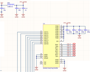
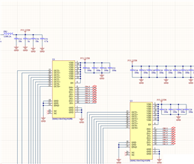
   Can you please suggest that if I can connect the NC pins 23 and 24 of  DS90LV804 to GND?

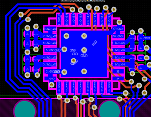
Also, can you please provide the reference layout for this IC. 

Many Thanks

Best Regards

Mohsin

  • Hi Mohsin,

    It is not recommended in the datasheet to connect NC pins 23 and 24 to ground. These pins are recommended to have no connection.

    We do not offer an EVM for this part to provide you as a reference layout, but if you provide a schematic we would be happy to review it for you.

    Thank you, Amy

  • Hi Amy, 

         Thank you for your quick reply. 

    Please find the Schematic circuit below. I need to use 4 of these buffer ICs and I am using an LDO of 700mA to power 4 ICs (140mA max per IC as per data sheet).   

    Can I also share the layout for review?

    Best Regards

    Mohsin

  • Hi Mohsin,

    Certainly, I am happy to review - thank you for providing.

    Here are a few comments:

    1) This device accepts LVDS/CML/LVPECL inputs. Double check that the input source meets the VIH/VIL requirements on datasheet page 3.

    2) I noticed the NC pins don’t have red “x” at the ends. I would recommend tying these to a “no connect” net.

    3) For the VDD pins: I realize the datasheet doesn’t provide any guidance on decoupling capacitors (and there are many VDD pins on this part). Please refer to this post. The poster has written many application notes for these devices over the years: DS90LV804: Decoupling capacitor for VDD pin

    4) I noticed the EN pin is tied high (perfectly fine). I just wanted to mention it to ensure that you are not interested in using the tri-state feature for the device. If so, be sure to add an option to tie this pin low.

    5) I realize this is just a schematic snip-it so I can't see the end of the bus, but ensure that the end of the bus is 100-ohm terminated (for each of the output pairs). Also be sure to check if the receiving device is internally terminated to avoid double termination. 


    Here are some general layout tips. Feel free to provide a layout file for review.

    1) As related to #5 above, be sure to place the 100-ohm termination resistor as close to the end of the bus as possible.

    2) As related to #1 it is recommended to place decoupling caps as close to the device pins as possible.

    Sincerely, Amy

  • Hi Amy,

           Thank you so much.

    1) This device accepts LVDS/CML/LVPECL inputs. Double check that the input source meets the VIH/VIL requirements on datasheet page 3.

    We are using an FPGA with LVDS output of 2.5V and I think this should be ok

    2) I noticed the NC pins don’t have red “x” at the ends. I would recommend tying these to a “no connect” net.

    I have fixed this 

    3) For the VDD pins: I realize the datasheet doesn’t provide any guidance on decoupling capacitors (and there are many VDD pins on this part). Please refer to this post. The poster has written many application notes for these devices over the years: DS90LV804: Decoupling capacitor for VDD pin 

    have gone through the document added the caps from large value to small and added one cap per pin of the device as shown, sorry can not share the full circuit therefore added a snap 


    4) I noticed the EN pin is tied high (perfectly fine). I just wanted to mention it to ensure that you are not interested in using the tri-state feature for the device. If so, be sure to add an option to tie this pin low.

    We do not need the Tri-state feature now 

    5) I realize this is just a schematic snip-it so I can't see the end of the bus, but ensure that the end of the bus is 100-ohm terminated (for each of the output pairs). Also be sure to check if the receiving device is internally terminated to avoid double termination. 

    The output of the device will be going to a cable assembly through a connector https://www.digikey.co.uk/en/products/detail/i-pex/81674-100B-02-D/22108870 which has an characteristic impedance of 84-87 ohm

    and the other end of cable is connected to a 2nd PCB with FPGA which has internal terminations. 

    a). Do I need to put termination resistors in this scenario on the connector? 

    b).  Do I need to consider anything else for PCB layout  - I am designing an eight layer board with 3 GND planes and one split power plane for 2.5V and 3.3V.  

    Any suggestions will be helpful, 

    Many Thanks

    Best Regards

    Mohsin

  • Hi Mohsin,

    1) You are correct, a 2.5V output is good, the signal will swing around a common mode of 1.25 V (LVDS standard is 1.2V CM but allows up to +/-1V ground shift).

    2), 3), 4) sounds good!

    5a) If the FPGA is 100-ohm internally terminated, be sure that an external termination resistor is not used (this would "doubly" terminate the bus). 

    5b) Decoupling cap placement looks great.  I have seen issues before with DC-DC converters coupling switching frequencies onto LVDS lines - you mentioned that you are using LDO's, so you should be fine, but I would recommend isolating any other sources of noise in the design to avoid coupling noise onto the differential pairs. Signal integrity is dependent on the data rate, cable type, and length. Since this is a four-channel device, you may consider differential length matching the four channel pairs. I really like the way this application note breakdown High-Speed Layout Guidelines, so I would use this as a reference / guide (Figure 4 is a nice diagram of intra-pair and inter-pair skew guidelines for differential signals). High-Speed Layout Guidelines for Reducing EMI for LVDS SerDes Designs (ti.com) I would recommend looking for ways to reduce the signal traces and cable length for signal integrity purposes. 

    Please let me know if you have any other questions! -Amy