Other Parts Discussed in Thread: TCA9517A, TCA9517, TCA9511A, TCA4307
FAQ: Logic and Voltage Translation > IxC >> What are the different I2C Buffer Direction Control Mechanisms?
I2C buffers implement direction control mechanisms to determine which side of the device is being driven LOW. This is crucial for any I2C buffer, since I2C is a bi-directional protocol requiring data to flow in both directions.
Static Voltage Offset
Devices: TCA9517, TCA9517A, TCA9509, TCA9617B
Static voltage offset is exactly as it sounds. A voltage that is static (unchanging), and represents some offset from GND. For reference, the static voltage offset on the TCA9517A is VOLB = 0.52V. This voltage offset is also known as a buffered LOW (see [FAQ] What is a buffered LOW?).
The static voltage offset (SVO) sets the output voltage (VOLB) of the buffer at a level higher than the input (VILC). This is to ensure that the buffer does not redrive its input from its own output voltage.

*Note that the VOL on B-side of the buffer is roughly 0.52V. The input voltage on B-side is a VILC = 0.45V. If the TCA9517A is driving a LOW from A-side to B-side, it will always output a voltage above the VILC which will prevent the buffer from propagating the LOW from B-side back to the A-side where the input signal originated.
Thus, we can understand the direction that the buffer is driving due to the output voltage on B-side. If the measured voltage is ~0.52V, we know that the buffer is driving from A-side to B-side.
If the voltage is <0.45V on B-side, then we can be confident that the buffer is propagating the LOW from B-side to A-side.
This is how a buffer with SVO propagates I2C signals bidirectionally without lock-up.
Current Mirror
Devices: TCA9800, TCA9801, TCA9802, TCA9803
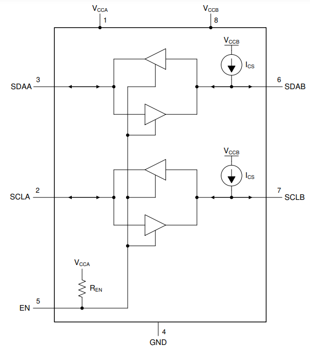
The TCA980x family of devices use a current mirror for direction control that detects the current pushing from the internal current source ICS or current that is being sunk. See the diagram of the internal structure of the TCA980x.

The benefit of using the current mirror over a static voltage offset is that the current mirror can push the VOL much lower than the SVO. See the electrical characteristics of the TCA980x in the table below.

See that VOLB = 0.22 V (typ.). This is much lower than the VOLB of the TCA9517/A at 0.52V. A lower VOL means that the B-side supply can be used with 1.8V logic since VIL = 30% of VCC = 30% of 1.8V = 0.54 V.
With TCA9517/A, VCCB = 1.8V is not in spec since the SVO can reach voltages up to 0.6 V which is larger than the 30% of VCCB threshold for VIL.
Dynamic Offset
Dynamic offset is present only within our hot-swap buffers such as the TCA9511A or TCA4307 (p2p to 9511A but w/ stuck bus recovery).
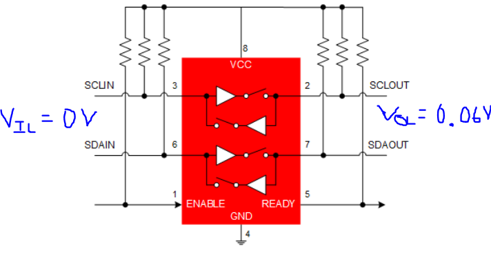
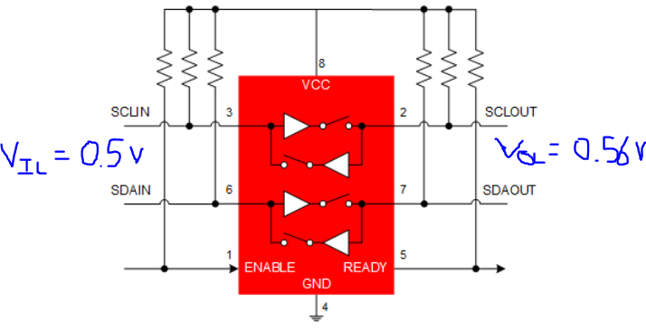
Dynamic offset is a changing voltage offset that occurs across the buffer. For example if a low voltage input on SDAIN/SCLIN is a VIL = 0V, then its output voltage on SDAOUT/SCLOUT would be VOL = VIL + 60mV.

The offset voltage is "dynamic" because it changes depending on the input. Now if VIL = 0.5V, the VOL = VIL + 0.06V = 0.56 V, a much larger offset!

This offset voltage also stacks with buffers that are stacked in series. For example, if 4 x TCA9511A's were stacked in series and VIL = 0V, the VOL at the slave/target device would be...
VOL = VIL + 4 x VOS =
VOL = 0V + 4 x 60mV = 0.24 V
VOS is the offset voltage. This is found in the datasheet underneath the electrical specifications for the TCA9511A and TCA4307.

Direction control is determined by the offset voltage. The buffer is smart enough to identify which direction the low is being propagated based off the offset voltage level.

