This thread has been locked.

If you have a related question, please click the "Ask a related question" button in the top right corner. The newly created question will be automatically linked to this question.

TIC12400-Q1: Some register writes/reads are not giving expected results

Part Number: TIC12400-Q1

Tool/software:

Hi,

We are using TIC12400-Q1 MSDI through SPI for one of our products on iMX8 running on Linux 6.6. We have referred datasheet and tried to configure registers
through spidev interface. But we are observing that some registers are configured succesfully but some are failing. When a write and then
read is performed on the same register, we get different values. This is observed for some of registers only. For example, when THRES_COMP register is
configured for 4V for all inputs.

Write -
root@imx8mp-falcon:~# spidev_test -v -D /dev/spidev2.0 -H 0 -b 32 -p "\xFE\x1F\x00\xA2"
[14336.987180] setup mode 1, cs_high, 32 bits/w, 1000000 Hz max --> 0
[14337.004606] setup mode 1, cs_high, 32 bits/w, 1000000 Hz max --> 0
[14337.022013] setup mode 1, cs_high, 32 bits/w, 500000 Hz max --> 0
spi mode: 0x1
bits per word: 32
max speed: 500000 Hz (500 kHz)
TX | FE 1F 00 A2 __ __ __ __ __ __ __ __ __ __ __ __ __ __ __ __ __ __ __ __ __ __ __ __ __ __ __ __ |....|
RX | 01 00 00 22 __ __ __ __ __ __ __ __ __ __ __ __ __ __ __ __ __ __ __ __ __ __ __ __ __ __ __ __ |..."|

Read -
root@imx8mp-falcon:~# spidev_test -v -D /dev/spidev2.0 -H 0 -b 32 -p "\x00\x00\x00\x22"
[14483.315089] setup mode 1, cs_high, 32 bits/w, 1000000 Hz max --> 0
[14483.332530] setup mode 1, cs_high, 32 bits/w, 1000000 Hz max --> 0
[14483.349950] setup mode 1, cs_high, 32 bits/w, 500000 Hz max --> 0
spi mode: 0x1
bits per word: 32
max speed: 500000 Hz (500 kHz)
TX | 00 00 00 22 __ __ __ __ __ __ __ __ __ __ __ __ __ __ __ __ __ __ __ __ __ __ __ __ __ __ __ __ |..."|
RX | 01 00 00 22 __ __ __ __ __ __ __ __ __ __ __ __ __ __ __ __ __ __ __ __ __ __ __ __ __ __ __ __ |..."|

But some of register write like CS_SELECT (0x1C), Mode (0x32), Device Id (0x1) are success.

So can you pls inform what can be possibel reason here. Let me know if you need more info.

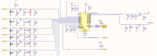
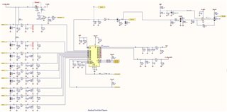
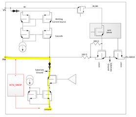
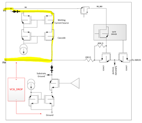
Attaching screenshot of the circuit here.

  • Hi Prashant,

    Can you share the full provisioning sequence attempt for every register in your initialization sequence? 

    The most likely issue is that you are setting the TRIGGER bit in the CONFIG register (0x1A[11] = 1) before you have completed the configuration of all of the device registers.  Once the TRIGGER bit is set, the other configuration registers become read only and the device starts the polling sequence on the INx pins.  If the TRIGGER bit is getting set to 1 before your configuration is complete, the registers will not accept the new write value and will return the value of the register at the moment the TRIGGER bit was set to 1 during a Read.

    Another possible reason could be SPI Errors on some of the SPI Writes to certain registers, possibly from a parity error which could cause the device to reject the new value of the register and retain the previous value.  Checking the format and byte values of the registers that return incorrect values could determine if this is a possible cause.  You could also try to do a read to the INT_STAT register after every SPI write and read to any other register to check for possible SPI and Parity errors as a debug tool.

    Regards,

    Jonathan

  • Thanks. It helped

    Can you pls share steps to configure a pin as Analog Input. And read the voltage.

  • Hi Prashant,

    I would first recommend reviewing the Steps to Configure TIC12400-Q1 Multiple Switch Detection Interface (MSDI) Application Note (Link).

    It provides a more step-by-step approach to configuring the device settings, including the ADC.  If you still have specific questions that aren't addressed in this application note, let me know.

    Regards,

    Jonathan

  • Hi Jonathan,

    Thanks.

    We tested the IC for Comparator Mode and it works.

    Now we are trying to configure bit IN10 line for ADC mode. The sequence followed for initialization is same as in flow chart of the sheet.
    I am pasting it below for ref. But we do not see Interrupt coming when the input voltage crosses threshold value. Pls inform what can be issue.

    1

    INT_STAT

    0x02


    spidev_test -v -D /dev/spidev2.0 -H 0 -b 32 -p "\x00\x00\x00\x04"

    2

    MODE - ADC (10)

    0x32

    Write

    spidev_test -v -D /dev/spidev2.0 -H 0 -b 32 -p "\x00\x08\x00\xE4"

    3

    WC_CFG0 - Wetting current (0)

    0x1D

    Write

    spidev_test -v -D /dev/spidev2.0 -H 0 -b 32 -p "\x00\x00\x00\xBA"

    4

    IN_EN - All channels

    0x1B

    Write

    spidev_test -v -D /dev/spidev2.0 -H 0 -b 32 -p "\x01\x08\x00\xB6"

    5

    INT_EN_CFG0 - Enable All types Interrupts

    0x24

    Write

    spidev_test -v -D /dev/spidev2.0 -H 0 -b 32 -p "\xFE\x1F\x00\xC8"

    6

    INT_EN_CFG1 - ADC Input Interrupt Gen (10)

    0x25

    Write

    spidev_test -v -D /dev/spidev2.0 -H 0 -b 32 -p "\x00\x08\x00\xCA"

    7

    THRES_CFG0 - 3v (after res calc) - 0x1FE

    0x29

    Write

    spidev_test -v -D /dev/spidev2.0 -H 0 -b 32 -p "\xFD\x03\x00\xD2"

    8

    THRESMAP_CFG1

    0x2F

    Write

    spidev_test -v -D /dev/spidev2.0 -H 0 -b 32 -p "\x00\x00\x00\xFE"

    9

    CONFIG - Trigger, CRC

    0x1A

    Write

    spidev_test -v -D /dev/spidev2.0 -H 0 -b 32 -p "\x01\x14\x00\xB4"

    10

    IN_STAT_ADC0 - Read Switch status

    0x6

    Read

    spidev_test -v -D /dev/spidev2.0 -H 0 -b 32 -p "\x01\x00\x00\x0C"

    11

    Interrupt Status

    0x02

    Read

    spidev_test -v -D /dev/spidev2.0 -H 0 -b 32 -p "\x00\x00\x00\x04

    But Read Switch Status always high for that line.

    root@imx8mp-f:~# spidev_test -v -D /dev/spidev2.0 -H 0 -b 32 -p "\x01\x00\x00\x0C"
    [  913.559201] setup mode 1, cs_high, 32 bits/w, 1000000 Hz max --> 0
    [  913.568254] setup mode 1, cs_high, 32 bits/w, 1000000 Hz max --> 0
    [  913.594067] setup mode 1, cs_high, 32 bits/w, 500000 Hz max --> 0
    spi mode: 0x1
    bits per word: 32
    max speed: 500000 Hz (500 kHz)
    TX | 01 00 00 0C __ __ __ __ __ __ __ __ __ __ __ __ __ __ __ __ __ __ __ __ __ __ __ __ __ __ __ __  |....|
    RX | 00 08 00 00 __ __ __ __ __ __ __ __ __ __ __ __ __ __ __ __ __ __ __ __ __ __ __ __ __ __ __ __  |....|

  • Hi Prashant,

    If I am decoding your SPI byte sequence correctly for your INT_EN_CFG1 register (0x25), it looks like you are setting a register value of 0x000400.  Bits 21-20 of this register are therefore set to "00" which is the setting for "no interrupt generation for IN10".

    I'm not sure your THRESMAP_CFG1 register configuration is correct.  I think you are trying to configure this register with a value of 0x000080 that would correspond with setting assigning THRES2 to the THRESMAP_IN10 field.  I think that would make your byte sequence "\x00\x01\x00\xDE"

    Regards,

    Jonathan

  • Thanks Jonathan. ADC mode is working.

    As informed in the previous messages, we are using IN10 for ADC. Can you pls share me the sequence for Voltage measurment.

  • Hi Prashant,

    I'm not sure I understand what voltage measurement you are asking about.  If you asking how to calculate the voltage from the ADC code, then the calculation will be:

    ADCcode = VINX x 1024 ÷ 6

    Regards,

    Jonathan

  • Thanks. Able to read voltage on ADC pin's.

  • Great! I'm glad it's now working for you.  Thanks for letting me know.

    Regards,

    Jonathan

  • Hi Jonathan,

    We are seeing one more issue.

    When configured in Comparator Mode, we are able to see interrupt generated only when wetting current is set to 0 mA.
    When wetting current is configured to any other non-zero value, interrupt is not generated when input voltage on the lines crosses threshold.
    Can you pls inform what can be possible reason here.

  • Hi Prashant,

    If you can provide the device register configuration you are now using and a schematic representation of the switch circuit you are connecting to the input pins, I can take a look.

    Regards,

    Jonathan

  • Hi Prashant,

    Just to clarify, I see the schematic from an earlier post, but it does not show the switches. It would be helpful to see the full path the wetting current would flow through.

    Regards,

    Jonathan

  • Hi Jonathan,

    Attaching screenshot from the schematics we have. Pls let me know if this is Ok or you need any other info.

  • Hi Prashant,

    Your schematic only shorts off-sheet port connectors.  Are there any additional components in the current path not shown in the schematic image you have provided?  Are you using physical switches and if so, are they connected to GND? 

    Regards,

    Jonathan

  • Hi Jonathan,

    Switch input lines are connected to Physical switches on other side. We are testing by setting these physical switches to high and then reading status and interrupt.

    Attaching the connector page of the schematic. Pls let me know if this clarifies.

  • Hi Prashant,

    Thank you for the additional information on the switches.  I was not aware you were using a high side switch configuration.  This will require the device to be in Current Sink mode which is configured in the CS_SELECT register 0x1C.  This register value was not in your previous post, and you didn't provide me with updated values, so I'm assuming you are leaving it at the default value which is set for Current Source mode which requires a low side switch configuration (switch to ground).

    If you are in Current Source mode, then the device will source current from the VS supply out of the INx pin.  If you are in Current Sink mode, the device will sink current into the INx pin to GND.

    If you have a high-side switch connected to the INx pin, and you are in Current Source mode, then there will be not be a good path to GND for the wetting current to flow and and the INx pin voltage will stay above the detection threshold.

    Please confirm your register configuration and I would also suggest you verify the actual pin voltages on a scope to make sure they are reaching the levels you expect.

    Regards,

    Jonathan

  • Hi Jonathan,

    Sry, for not sharing the updated sequence for Comparator Mode. We are configuring CS_SELECT in Battery Mode i.e CSI. Below is the sequence used.

    1

    INT_STAT - Interrupt Status

    0x02

    Read

    spidev_test -v -D /dev/spidev2.0 -H 0 -b 32 -p "\x00\x00\x00\x04"

    2

    MODE - Comparator

    0x32

    Write

    spidev_test -v -D /dev/spidev2.0 -H 0 -b 32 -p "\x01\x00\x00\xE4"

    3

    THRES_COMP - Threshold - 2V

    0x21

    Write

    spidev_test -v -D /dev/spidev2.0 -H 0 -b 32 -p "\x00\x00\x00\xC2"

    4

    CS_SELECT - Batt (CSI)

    0x1C

    Write

    spidev_test -v -D /dev/spidev2.0 -H 0 -b 32 -p "\xFE\x07\x00\xB8"

    5

    IN_EN - All channels

    0x1B

    Write

    spidev_test -v -D /dev/spidev2.0 -H 0 -b 32 -p "\xFE\xFF\xFF\xB7"

    6

    INT_EN_COMP1 - Switch Int1

    0x22

    Write

    spidev_test -v -D /dev/spidev2.0 -H 0 -b 32 -p "\xFE\xFF\xFF\xC5"

    7

    INT_EN_COMP1 - Switch Int2

    0x23

    Write

    spidev_test -v -D /dev/spidev2.0 -H 0 -b 32 -p "\xFF\xFF\xFF\xC7"

    8

    INT_EN_CFG0 - Enable All Int

    0x24

    Write

    spidev_test -v -D /dev/spidev2.0 -H 0 -b 32 -p "\xFE\x1F\x00\xC8"

    9

    WC_CFG0 - Wetting Curr

    0x1D

    Write

    spidev_test -v -D /dev/spidev2.0 -H 0 -b 32 -p "\x00\x00\x00\xBA"

    10

    CONFIG - Debounce

    0x1A

    Write

    spidev_test -v -D /dev/spidev2.0 -H 0 -b 32 -p "\x01\x80\x01\xB4"

    11

    CONFIG - Trigger

    0x1A

    Write

    spidev_test -v -D /dev/spidev2.0 -H 0 -b 32 -p "\x01\x14\x00\xB4"

    12

    IN_STAT_COMP - Read switch status

    0x5

    Read

    spidev_test -v -D /dev/spidev2.0 -H 0 -b 32 -p "\x01\x00\x00\x0A"

    13

    Interrupt Status

    0x02

    Read

    spidev_test -v -D /dev/spidev2.0 -H 0 -b 32 -p "\x00\x00\x00\x04"

    Sharing other wetting current commands.


    Wetting curr to 1

    0x1D

    spidev_test -v -D /dev/spidev2.0 -H 0 -b 32 -p "\x92\x24\x49\xBA"


    Wetting curr to 2


    spidev_test -v -D /dev/spidev2.0 -H 0 -b 32 -p "\x24\x49\x92\xBA"


    Wetting curr to 5


    spidev_test -v -D /dev/spidev2.0 -H 0 -b 32 -p "\xB6\x6D\xCB\xBA"


    Wetting curr to 10


    spidev_test -v -D /dev/spidev2.0 -H 0 -b 32 -p "\x48\x92\x24\xBB"


    Wetting curr to 15


    spidev_test -v -D /dev/spidev2.0 -H 0 -b 32 -p "\xFE\xFF\xFF\xBB"

    We checked input voltages and observed that input voltages remain high for higher wetting currents (i.e for non-zero wetting currents). Sharing below values measured on line-0 and line-1. What can be the reason ?.

    Wetting curr
    (mA)

    Line 0 (Low)
    (volts)

    Line 1 (High)
    (volts)

    0

    0

    21.7

    1

    20.95

    21.7

    2

    20.96

    21.7

    5

    20.95

    21.7

  • Hi Prashant,

    The basic operating principle of these devices is simply Ohm's Law (V = I*R), so the voltage level is based on the voltage drop across the resistance with some amount of current.

    With Current Source configurations, GND or 0V is the "fixed" voltage reference and the resistance is located between GND and the INx pin.  Therefore the INx pin voltage is always the product of the voltage drop across the resistance (Vinx = I*R).

    However, with Current Sink configurations, the resistance sits between the Supply Voltage and the INx pin, so the Supply voltage becomes the "fixed" voltage reference.  The INx pin voltage is then the voltage drop across the resistance subtracted from the Supply voltage. (Vinx = Vs - (I*R))

    From your schematic you have a 100 ohm series resistor, so even at the maximum wetting current threshold of 15mA, the maximum voltage drop across this 100 ohm resistor is 1.5V.  Therefore your INx pin voltage will only be 1.5V less than your supply voltage.  With Current Sink configurations, you need a much larger series resistance in order to create a voltage drop large enough to drop the voltage below the comparator or ADC voltage threshold.

    I also have a question or concern about the 21V to 22V levels you have.  What is the supply voltage you are using?  The TIC12400-Q1 is a 12V device and is tolerant of voltage levels up to 35V, but should not be operated with a steady voltage of greater than 16V.  Operation greater than 16V can reduce the lifespan of the device in some devices, so it should only be used in 12V systems.

    Regards,

    Jonathan

  • Hi Jonathan,

    Thanks for the info.

    • So, I believe the sequence followed for comparator is correct, right ?.

    • In CSI mode during switch open condition, we are observing voltage of 21v at INx pins when wetting current is set to non-zero values.
      IC chip should be sourcing voltage only in current source mode and not in current sink mode. Pls confirm.

                   So, question is why high voltage(i.e 21v) is seen on INx pins during CSI mode when wetting currents are high ?.

  • Hi Prashant,

    For the 5mA configuration, IN0_IN1 current level seems to be set to 0mA and the IN10 current level seems to be set to 1mA with your values.  Otherwise your SPI sequence looks correct for comparator mode with 2V thresholds and current sink mode.

    I also have a question or concern about the 21V to 22V levels you have.  What is the supply voltage you are using? 

    Here is a simplified representation of how the device works with respect to the current source, sink, and internal MUX.  The device operates more like a current limiter and will source or sink current up to the configured wetting current level.  However, Ohm's Law is the general principle and therefore the voltage level on the INx pin will depend on the external resisitive load.  The device will not "force" a constant current level and because the maximum voltage level is the VS supply or battery voltage, large resistive loads may result in lower levels of current.

    In the case of the current sink configuration, there is a low impedance path created through the FETs located between the INx pin and GND.  Because these FETs sit between GND and the INx pin, there is some voltage drop which forces the minimum INx pin voltage to a >0V level as specified in the datasheet.  However, the device will not place 21V on the INx pin, and this level must be coming from an external source.

    In the Current Source configuration, a low impedance path is created between the VS supply pin and the INx pin.  Therefore the largest voltage that can be placed on the INx pin is a diode's drop (0.6V) less than the VS supply voltage.

    In the 0mA configuration, there is some leakage current that will flow through the MUX circuit (specified in the datasheet as +/- 110uA) which is only present when that particular INx channel is actively connected to the Comparator or ADC for sampling (18-24us).  If the external circuitry on the INx pin does not provide a low impedance path to GND or have enough filter capacitance to absorb this current, it can momentarily pull the INx pin high and add some error to the voltage being sampled.  However, the 0.1uF caps and external circuit you have on each pin should prevent the INx pin from seeing a large voltage on this pin in the 0mA case.

    In current sink mode, the maximum voltage seen on the INx pin without an external source is Vcsi_drop which has a max level of 2.1V (much lower than 21V).  Therefore I would check for an external source that is pulling the INx pin to this high voltage.

    Regards,

    Jonathan

  • Hi Jonathan,

    Thanks for the detailed explanation.

    • At CSO mode, is there a way to add internal pull-up resistor for 0 mA wetting current?

    •  We are also validating ADC mode on pin-10. Interrupts are generated only when wetting current is 0mA. For higher wetting currents no interrupts are generated. Sharing the sequence below. Pls provide your suggestion.

    spidev_test -v -D /dev/spidev2.0 -H 0 -b 32 -p "\x00\x00\x00\x04" - INT_STAT
    spidev_test -v -D /dev/spidev2.0 -H 0 -b 32 -p "\x00\x08\x00\xE4" - MODE - ADC (10 line)
    spidev_test -v -D /dev/spidev2.0 -H 0 -b 32 -p "\x00\x00\x00\xBA" - Wetting Curr 0mA
    spidev_test -v -D /dev/spidev2.0 -H 0 -b 32 -p "\xFE\xFF\xFF\xB7" - IN_EN All channels
    spidev_test -v -D /dev/spidev2.0 -H 0 -b 32 -p "\xFE\x1F\x00\xC8" - INT_EN_CFG0 - Enable all
    spidev_test -v -D /dev/spidev2.0 -H 0 -b 32 -p "\x01\x00\x60\xCA" - INT_EN_CFG1 - ADC Input Interrupt Gen (10)
    spidev_test -v -D /dev/spidev2.0 -H 0 -b 32 -p "\xA4\x06\x00\xD2" - THRES_CFG0 19.5v
    spidev_test -v -D /dev/spidev2.0 -H 0 -b 32 -p "\x00\x14\x04\xB4" - CONFIG - Trigger, CRC, VS_MEAS_EN
    spidev_test -v -D /dev/spidev2.0 -H 0 -b 32 -p "\x00\x00\x00\x04" - INT_STAT

  • Hi Prashant,

    No, there is not a way to add an internal pull-up resistor.  The wetting current is effectively the same as adding a pull-up resistor.  You would need to add any required pull-up resistors externally.

    I will try to take a look at your sequence using an EVM.

    Regards,

    Jonathan

  • Hi Prashant,

    Your notes say 19.5V for THRES_CFG0, but please note the ADC only has a 0V to 6V range.  Therefore, you are configuring an ADC interrupt threshold of approximately 4.98V.  Is this the threshold voltage you want?  I don't understand the 19.5V note.

    Can you measure and verify the actual voltage on the IN10 pin to ensure it is crossing above and below 4.98V?

    Regards,

    Jonathan