This thread has been locked.

If you have a related question, please click the "Ask a related question" button in the top right corner. The newly created question will be automatically linked to this question.

TLIN1431-Q1: TLIN1431-Q1

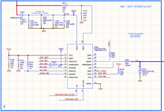
Part Number: TLIN1431-Q1

Tool/software:

BCI.docx

Hello,BCI.docx

I am currently used TLIN14315 in an automotive project.

We have performed BCI (bulk current injection ) tests. 

Short document for BCI test included in the documents .

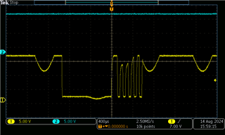
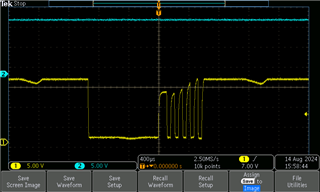
In the BCI (Bulk current injection) test we have an interesting behavior of the LIN driver.

When the LIN line is disconnected from the master during BCI test the inside low side MOS transistor from TL14315 start conducting because of the signal from the drain(our presumption).

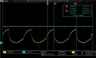
When the LIN is connected with the master we have communication timeouts

Could you help us to understand the this behavior and possible ways of solving ?

Thank you

Marian

  • Marian,

    Thanks for reaching out! Generally, BCI performance is a big factor of layout. From looking at your schematic, it appears that you have a good amount of filtering on the input supply, so it could be helpful to look for ways to ensure very strong grounding in your board layout. Try to make sure that the incoming AC energy passes the filtering components before it is able to reach the transceiver, and that you have a small decoupling capacitor placed near the input supply pin to the device itself.

    In the document you attached, it mentioned Level 2 acceptance criteria for this BCI test. What is the error behavior that meets Level 2 acceptance?

    Best,

    Danny

  • Hello Danny,

    This is the layout .We have a strong grounding for the filtering components.

    Level 2 is the magnitude of the current injected on the coil.

    The acceptance criteria is that the ECU should not have any errors during the test.

    In this picture is the setup .

    I look forward for new ideas about this issue

    Thank you

    Marian

  • Marian,

    My apologies for the delay - I had thought that I'd responded here but it looks like I dropped it on my end.

    Thanks for the additional layout information, it's helpful to see. From what it looks like, I believe you and your team have put together a strong schematic and layout. I do have one item that I'd like to check, and also some additional questions.

    As the one item to check, could you try this without the diode to see whether your performance changes? (We expect no change, but just want to be sure.)

    And also, just a few questions to help make sure we're understanding your tests.

    For the two images you included, do I understand that the image on the left is without master connected, while the image on the right is with master connected? Based on what you described, it sounds like the responder/slave is adding an additional dominant pulse/bit, but just want to be sure. I see a sync field in both of the images.

    Also, in my experience, I've seen many cases where immunity test conditions are that there cannot be more than 4 consecutive errors in LIN communication. Is there an error limit (>1) for your testing?

    Best,

    Danny

  • Hello Danny,

    Thank you for the answer.

    The image without master connected (measured at slave board) is the following:


    The other 2 images are with the master connected during the BCI test.

    BCI test consist in a wireless injection (with a coil)of a sine wave that is AM modulated.

    About the diode , do you refer to the ESD diode (D202)?

    We have made some test also without D202 but with the same behavior.

    The LIN cable from slave(in the anechoic chamber)and master is about 10 meters.

    A second pull up placed closed to the slave (1.2m) can be improve behavior ?

    Thank you

    Marian

  • Marian,

    Apologies for the delay here - we're still working on getting this for you and should be able to get you a response by tomorrow Central time (USA).

    Best

    Danny

  • Hello Danny,

    This issue is urgent and until now we tried few 'workarounds" (like common mode choke)but without success.

     The project is in a status that we did not have much time.

    Could you help us ?

    Thank you

    Marian

  • Marian,

    Our team has been working to try and get some feedback for your use case that might explain the phenomenon. We haven't observed this behavior in our lab before, and our standardized testing houses have not reported similar communication issues during testing.

    The BCI testing that's done at UL, for example, has shown this device passing without any performance deviations during the test (across all device modes/states).

    Also, from looking at your test setup photo, I'm not able to see any major points of concern that arise suspicion.

    So, given this, I'm left to look toward the PCB for root causes.

    You mention that you used a common-mode choke - by this, do you mean a ferrite bead L201?

    I noticed that the TXD pin does not have decoupling shown on the schematic. Is there a way for you to try and add some slight decoupling capacitance on this line in your lab to see whether the performance is changed? It would only need to be something small, perhaps a few picohms.

    Best,

    Danny

  • Hello Danny,

    Thank you for your answer.

    Could you  please send us some details about the test setup and condition of the test you have performed.

    Maybe there are some think that we did not made correctly on the setup.

    Also a test report will be welcomed.

    The common mode choke that we have tried to use was placed outside the board .

    The common mode choke was placed between VBAT and LIN. 

    The results was better with the common mode choke that without - the current read by the second coil from setup was smaller but not small enough.

    Also we have decrease the injected current in the BCI coil to 50mA (from 200mA required by the client) and the test passes.

    Best regards

    Marian