This thread has been locked.

If you have a related question, please click the "Ask a related question" button in the top right corner. The newly created question will be automatically linked to this question.

DS90UB941AS-Q1: How to display from DSI input

Part Number: DS90UB941AS-Q1

Tool/software:

Hi expert,

I have asked about using UB941 and UB948 before,

DS90UB941AS-Q1: How to config register to connect 948 with DOUT0? - Interface forum - Interface - TI E2E support forums

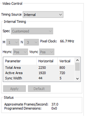
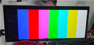
and with the configuration provided by TI's experts, it is already possible to display color pictures without DSI input by configuring the SER PG.

here is the result and the configuration:

[MCU2_0] 11.183765 s: Read 941 device id at 0xc, I2C ID Reg[0x0000] = 0x18
[MCU2_0] 11.183793 s: ----write UB941-----
[MCU2_0] 11.184018 s: After write, read I2c address at 0xc, I2C ID Reg[0x0001] = 0x0
[MCU2_0] 11.184507 s: After write, read I2c address at 0xc, I2C ID Reg[0x0001] = 0x8
[MCU2_0] 11.185507 s: After write, read I2c address at 0xc, I2C ID Reg[0x0003] = 0xda
[MCU2_0] 11.186506 s: After write, read I2c address at 0xc, I2C ID Reg[0x005b] = 0x0
[MCU2_0] 11.187506 s: After write, read I2c address at 0xc, I2C ID Reg[0x001e] = 0x1
[MCU2_0] 11.188505 s: After write, read I2c address at 0xc, I2C ID Reg[0x0066] = 0x1a
[MCU2_0] 11.189505 s: After write, read I2c address at 0xc, I2C ID Reg[0x0067] = 0x1
[MCU2_0] 11.190505 s: After write, read I2c address at 0xc, I2C ID Reg[0x0066] = 0x3
[MCU2_0] 11.191505 s: After write, read I2c address at 0xc, I2C ID Reg[0x0067] = 0x3
[MCU2_0] 11.192505 s: After write, read I2c address at 0xc, I2C ID Reg[0x0066] = 0x4
[MCU2_0] 11.193505 s: After write, read I2c address at 0xc, I2C ID Reg[0x0067] = 0xca
[MCU2_0] 11.194505 s: After write, read I2c address at 0xc, I2C ID Reg[0x0066] = 0x5
[MCU2_0] 11.195505 s: After write, read I2c address at 0xc, I2C ID Reg[0x0067] = 0x8
[MCU2_0] 11.196505 s: After write, read I2c address at 0xc, I2C ID Reg[0x0066] = 0x6
[MCU2_0] 11.197506 s: After write, read I2c address at 0xc, I2C ID Reg[0x0067] = 0x32
[MCU2_0] 11.198505 s: After write, read I2c address at 0xc, I2C ID Reg[0x0066] = 0x7
[MCU2_0] 11.199505 s: After write, read I2c address at 0xc, I2C ID Reg[0x0067] = 0x80
[MCU2_0] 11.200509 s: After write, read I2c address at 0xc, I2C ID Reg[0x0066] = 0x8
[MCU2_0] 11.201506 s: After write, read I2c address at 0xc, I2C ID Reg[0x0067] = 0x7
[MCU2_0] 11.202505 s: After write, read I2c address at 0xc, I2C ID Reg[0x0066] = 0x9
[MCU2_0] 11.203505 s: After write, read I2c address at 0xc, I2C ID Reg[0x0067] = 0x2d
[MCU2_0] 11.204505 s: After write, read I2c address at 0xc, I2C ID Reg[0x0066] = 0xa
[MCU2_0] 11.205505 s: After write, read I2c address at 0xc, I2C ID Reg[0x0067] = 0x2c
[MCU2_0] 11.206505 s: After write, read I2c address at 0xc, I2C ID Reg[0x0066] = 0xb
[MCU2_0] 11.207505 s: After write, read I2c address at 0xc, I2C ID Reg[0x0067] = 0x5
[MCU2_0] 11.208505 s: After write, read I2c address at 0xc, I2C ID Reg[0x0066] = 0xc
[MCU2_0] 11.209505 s: After write, read I2c address at 0xc, I2C ID Reg[0x0067] = 0xad
[MCU2_0] 11.210505 s: After write, read I2c address at 0xc, I2C ID Reg[0x0066] = 0xd
[MCU2_0] 11.211505 s: After write, read I2c address at 0xc, I2C ID Reg[0x0067] = 0x38
[MCU2_0] 11.212505 s: After write, read I2c address at 0xc, I2C ID Reg[0x0065] = 0x4
[MCU2_0] 11.213505 s: After write, read I2c address at 0xc, I2C ID Reg[0x0064] = 0x15
[MCU2_0] 11.214505 s: After write, read I2c address at 0xc, I2C ID Reg[0x001e] = 0x1
[MCU2_0] 11.215505 s: After write, read I2c address at 0xc, I2C ID Reg[0x0007] = 0x58
[MCU2_0] 11.216505 s: After write, read I2c address at 0xc, I2C ID Reg[0x0008] = 0x5c
[MCU2_0] 11.217505 s: After write, read I2c address at 0xc, I2C ID Reg[0x0001] = 0x0
[MCU2_0] 11.718604 s: Read 948 device id at 0x2c, I2C ID Reg[0x0000] = 0x58
[MCU2_0] 11.718631 s: ----write UB948ONE-----
[MCU2_0] 11.718909 s: After write, read I2c address at 0x2c, I2C ID Reg[0x0049] = 0x60
[MCU2_0] 11.973565 s: After write, read I2c address at 0x2c, I2C ID Reg[0x001d] = 0x13
[MCU2_0] 12.228568 s: After write, read I2c address at 0x2c, I2C ID Reg[0x001e] = 0x55
[MCU2_0] 12.483567 s: After write, read I2c address at 0x2c, I2C ID Reg[0x001f] = 0x5
[MCU2_0] 12.738300 s: DSS: SERDES Configuration... Done !!!

so how do I transfer the data via DSI and display it on the screen next?

  • Hi Xuefei,

    Thank you for providing your PATGEN code and linking the previous E2E thread.

    so how do I transfer the data via DSI and display it on the screen next?

    There will be additional setup required for the DSI input

    • TSKIP_CNT (Section 8.3.1.2)
    • Number of DSI Lanes (MainPage register 0x4F, also a strap option)
    • Continuous or non-continuous DSI clock (MainPage register 0x56)
    • If using DSI sync events instead of sync pulses, additional config is required

    DSI frequency = PCLK * 12 / (Number of DSI lanes)

    This was the video timing I recorded from your 941 code. Is the PCLK correct? Can you confirm the number of DSI lanes, continuous or non-continuous DSI clock, and sync events?

    Once we get this info, I can help generate an example initialization script.

    Best,

    Jack

    I have attached an example 941 config script. Based off of your PATGEN timing, the 

  • The PCLK I calculated by the formula is 108Mhz and what I see from the picture you get is 66.7Mhz.

    Does this have anything to do with the values of M and N? What should M and N be set?


    The configuration I need is shown below

    HT

    2250

    VT

    800

    HA

    1920

    VA

    720

    HS

    44

    VS

    5

    HFront

    113

    VFront

    19

    HBack

    173

    VBack

    56

    refresh_rate

    60

    PCLK

    2250 * 800 * 60= 108000000

    DSI lanes

    4

    DSI clock

    continuous

    sync

    pulses


    Please help me generate an example initialization script based on the above information, thank you.


    Also, I'm not quite sure the difference between sync events and sync pulses, can you explain that to me?

  • I would also like to ask, is the DSI input you mentioned only achievable via the configuration register?
    I want to input the image generated by the camera or GUI library to the display via DSI.
    I'm using the RTOS0902 SDK, so does it involve storing the image data generated by the camera or GUI library into a buffer like a frame buffer, and then transferring it to the screen through the DSI send interface?

  • Hi Xuefei,

    Thank you for providing the video resolution and DSI information.

    Also, I'm not quite sure the difference between sync events and sync pulses, can you explain that to me?

    Sync pulses rely on start and end packets to define timing for horizontal and vertical sync width.

    Sync events only send start packets for horizontal and vertical syncs. See datasheet section 8.4.2.2.1 for info.

    Does this have anything to do with the values of M and N? What should M and N be set?

    When using PATGEN with internal timing, the values of M and N determine the calculated PCLK.

    Use M = 10, N = 74. This is not exactly 108MHz but I can only get so close.

    Please help me generate an example initialization script based on the above information, thank you.

    See attached script

    # Example 941AS config script
    
    serAddr = 0x18
    desAddr = 0x58
    
    board.WriteI2C(serAddr, 0x01, 0x08) # Disable DSI
    
    # Program TSKIP_CNT on DSI Port 0
    # DSI Port 0 = 324Mbps
    board.WriteI2C(serAddr, 0x40, 0x04)
    board.WriteI2C(serAddr, 0x41, 0x05)
    board.WriteI2C(serAddr, 0x42, 0x20) # TSKIP_CNT = 0x10
    board.WriteI2C(serAddr, 0x01, 0x00) # Enable DSI
    
    board.WriteI2C(serAddr, 0x3, 0x96) # Enable I2C pass-through

    I would also like to ask, is the DSI input you mentioned only achievable via the configuration register?
    I want to input the image generated by the camera or GUI library to the display via DSI.

    My expertise only applies to the UB941AS. Please contact the engineers of the SoC you are using for help with sending DSI data.

    Best,

    Jack

  • Hi Xuefei,

    Below is a link to the "DS90UB941AS-Q1 DSI Bringup Guide" app note. This is a very helpful app note for resolving DSI issues that arise when using the UB941AS.

    https://www.ti.com/lit/an/snla356/snla356.pdf?ts=1730859596873&ref_url=https%253A%252F%252Fwww.google.com%252F

    Best,

    Jack

  • Will there be a picture on the screen in this configuration, according to this configuration, I need to modify 0x48 to the 0x3 to ensure that it can be connected to UB948, and it supports backlight, but I don't see any display screen now.

  • Hi Xuefei,

    The configuration I sent over does not use PATGEN. Do you want a PATGEN configuration?

    according to this configuration, I need to modify 0x48 to the 0x3 to ensure that it can be connected to UB948,

    Can you clarify this? I'm not sure what you mean by modify 0x48 to the 0x3.

    If there are any other configurations you need to turn on the backlight or other peripherals, add them as necessary.

    Best,

    Jack