- Ask a related questionWhat is a related question?A related question is a question created from another question. When the related question is created, it will be automatically linked to the original question.
Tool/software:
Hello:
The customer is using SN65DSI186ZXHR for the mid depth screen of EDP. Currently, there is a probability of screen flickering during sleep and wake-up, with the phenomenon of up and down jumping
Later, the FAE analysis of the screen module factory and TI chip did not provide a specific reason, but only tested the power on timing of the screen and TI. After testing, it was found that the timing did not match.
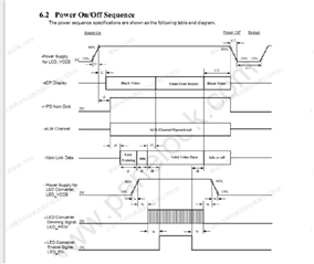
EDP screen power on timing
TXN0 and TXN1 are powered on first, with an interval of 2.74ms
After 3V3 is powered on, HPD is powered on with an interval of 83.6ms
After HPD is powered on, TXN0 and TXN1 are powered on again with an interval of 361.4ms
Note: TXN0 and TXN1 have a primary power on voltage of 0.308V and a secondary power on voltage of 0.468V
EDP screen sleep wake-up timing
TXN0 and TXN1 are powered on first, followed by 3V3, with an interval of 29.8ms. They should be kept away from the startup interval of 2.74ms. After 3V3 is powered on, TXN0 and TXN1 are powered on again, with an interval of 63.44ms
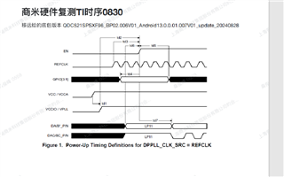
The timing sequence tested by the customer is below
Modify the power on timing according to the specifications provided by the module factory, then turn off the PLL enable when suspending, and turn it back on when powering on. After testing thousands of times, no problems have been found temporarily.
However, during reliability testing, high temperature operation: after 72 hours of low-temperature storage and returning to room temperature for inspection, the problem of the main screen flashing occurred after 20 hours of high-temperature operation testing. In addition, it may also occur during normal use in the future, as well as during CIT and aging testing
Also, the value of the register printed when the screen flashes is F6=40 when there is a problem, and it is 0 when normal.
May I ask if there are any troubleshooting points to help customers with troubleshooting and analysis, and if there are any good suggestions,Thanks!!!