This thread has been locked.

If you have a related question, please click the "Ask a related question" button in the top right corner. The newly created question will be automatically linked to this question.

DP83825I: Clarification on RST_N Pin Pullup Voltage

Part Number: DP83825I


Tool/software:

Hi, 


I have a question about the DP83825I Ethernet PHY and the behaviour of its RST_N pin.


We are using the DP83825I in our design with a 1.8V VDDIO. However, we noticed that the RESET signal connected to the RST_N pin has a voltage level of 2.2V-2.5V instead of 1.8V.

According to the DP83825I datasheet, the RST_N pin should operate at the same voltage level as VDDIO. Could you please clarify the following

  • Is the internal pull-up resistor on the RST_N pin fixed at 3.3V or is it connected to VDDIO as stated in the datasheet?
  • If it is connected to VDDIO, are there any conditions under which this discrepancy could occur?


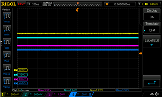
This behaviour is a key concern in our design, and resolving it is crucial to ensure proper operation. To help you understand the situation, I’ve attached two figures:

  • One showing the behaviour with the PHY connected.
  • The other shows the behaviour when the signal to the RST_N pin is disconnected.


Your advice on this matter would be greatly appreciated.


Thank you for your support!

  • Hi, 

    Thank you for submitting your query, I am happy to assist. 

    The internal pullup resistor for the RST_N pin is connected to the VDDIO voltage level of the PHY. 

    In order to narrow down why this behaviour is observed, I wanted to clarify a few things and make sure I am understanding the issue correctly

    1. Could you verify the voltage level seen on the VDDIO and AVDD pins of the PHY?
    2. Where are the voltages provided being read from? Ideally, we want to read these voltage at the PHY pin or as close to it as possible to get the most accurate readings.
    3. I see that the voltage is being driven at 1.8V by the SoC, but connecting it to the reset pin of the PHY makes it jump up to 2.5V. Is this understanding correct?
    4. Can you measure the voltage at the reset pin of the PHY with it being disconnected from the SoC driving the 1.8V?

    Best,

    Vivaan

  • Hi Vivaan,

    Thank you for your reply. I've addressed your points below to clarify the situation:

    1. VDDIO and AVDD measurements:
      The voltage levels on the VDDIO and AVDD pins of the PHY are correct, with VDDIO at 1.8V and AVDD at 3.3V. I verified this with direct measurements.
    2. Measurement points:
      I measured as close to the PHY pins as possible to ensure accuracy.
    3. Voltage behaviour at RST_N:
      Yes, your understanding is correct. This behaviour seems to be consistent with the information I found in another forum thread, which suggests that RST_N may be internally pulled to AVDD (3.3V) by the PHY. What voltage node is RST_N terminal internal pull up connected to?
    4. Voltage with RST_N disconnected:
      I also measured the voltages (VDDIO, AVDD, GRST(globale RESET) and PRST(phy RESET)) with the RST_IN pin disconnected. These measurements are included in the figure I've attached.

    Based on the measurements and the observed behaviour, it appears that RST_N has an internal pullup with AVDD. Can you confirm this? If further clarification is needed, I’d be happy to provide additional details.

    Best regards 
    Hamza

  • Hi Hamza,

    Thank you for providing the scope plots! After looking more into this, it seems like your observations are correct. We have an internal note that the reset pin is tied to AVDD and not VDDIO. This change will be addressed in the new datasheet revision for this product releasing soon. 

    Best, 

    Vivaan