


Part Number: DS90LV048A
Other Parts Discussed in Thread: DS90LV012A, SN74LVC1G04
Tool/software:
hi
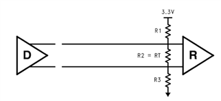
customer already study the app note (snla051c.pdf) for external biasing for failsafe.
But they are not able to figure out the reference resistor value.
Is there a reference resistor value for below circuit to be used together with DS90LV012ATMF to order to get a output LOW output during fail-safe?
Best Regards,
kpk

