This thread has been locked.

If you have a related question, please click the "Ask a related question" button in the top right corner. The newly created question will be automatically linked to this question.

TDES954: Layout Related queries for V3Link interface

Part Number: TDES954

Tool/software:

Hi Hamzeh,

We have following changes to V3Link layout as per below:

  1. RF trace reference layer changed to Layer-2 instead of Layer-3 which resulted in RF trace width decreased to 5.2mils.
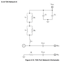
  2. Changed POC network from TDK Network-5 to TDK Network-6.

We have following queries:

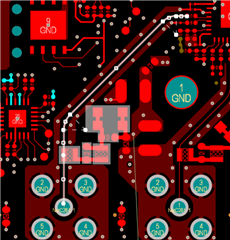
  1. As shown in below image, we have placed all POC network components on Top layer. Our RF engineer recommends placing all POC components except L3 in the bottom layer to improve RF performance and marginal test results.
  2. We have kept GND shield trace clearance around the RF trace 3W (15.6mils) far away each side and kept 4W (20.8mils) anti pad at RF TH pin for Fakra connector.

We would like to know your recommendations and inputs here to proceed further.

  • Hello,

    the team is out due to the Holidays. Responses will be delayed from Dec. 24 through Jan. 2.

    Thank you for your patience

  • Hello Nimesh,

    I don't have full visibility of the comments that were made in the previous revision of the layout, since much discussion seems to have taken place over email, but here are my thoughts after reading the previous E2E post and the screenshot you have provided.

    1) Do you have access to the Channel Specs document for these devices, or are aware of the Insertion Loss and Return Loss limits of these V3Link devices?

    2) Have you performed S-Parameter simulations on the high-speed RIN and DOUT traces on your PCBs?

    3) Have you optimized your layout for 50-Ohms controlled impedance on the high-speed RIN and DOUT traces?

    4) Would you like to request another layout review with your updated layout files?

    Best,

    Justin Phan

  • Hello Justin,

    Thank you for your reply.

    Please find our responses below:

    1. Yes, we have access to the Channel Specs document.

    2. Yes, we have conducted S-Parameter simulations on the RIN1+ trace using the existing PCB layout. Please see the attached image for the results.

    3. Yes, we have routed the RIN traces to maintain a 50-Ohm impedance.

    4. Yes, we would like to request to review of the modified layout where we have implemented the changes suggested by TI. Could you please share your email address so that we can add you in the email chain?

  • Hello Nimesh,

    My email is j-phan1@ti.com

    1) For those S-Parameter measurements, could you also elaborate on how you took them?

    2) Did you take the S-Parameter of only the PCB traces?

    3) Did you depopulate the FPD-Link IC and replace it with a 50-Ohms resistor to GND? And also use VNA probes? Or a soldered SMA cable?

    Best,

    Justin Phan

  • Received files over email and am now evaluating.

  • Latest update from email:

    It seems that IL and RL are failing the TDES954 limit lines at the frequency ranges above 1GHz, even without the PoC network populated. This means that either:

    1. Maybe the measurement setup is adding additional loss to the measurement results.
      1. Excess solder, maybe at the connector may be skewing the measurement results a bit.
    2. The PCB traces are particularly lossy at higher frequencies, so the failing loss results may not be related to the PoC network.
      1. In terms of Insertion Loss, what is the dielectric material being used and what is the Dk and Df values? If the material is lossy, then you may need to shorten the RIN+ trace, to compensate for the loss.
        1. There are also weird dips in the IL results from 10MHz – 100MHz. I suspected maybe a measurement setup error, but it is gone when you depopulate the PoC network.
      2. In terms of Return Loss, it seems you’re passing at the lower frequency range of around 25MHz, but you are failing at the upper frequencies at 1GHz. It seems the PoC network adds a marginal amount of RL at the upper frequencies, but the RL above 1GHz was already high on the PCB traces to begin with. Can you run a TDR from the connector to the RIN+ IC pin? With the AC coupling capacitor populated?
      3. It seems there is excess RL on the RIN+ trace itself. Maybe due to impedance mismatch somewhere?

    You can try some of the suggestions. And also reach out to TDK as well, to get their opinion on the PoC network they designed.