TLK10031: TLK10031

Part Number: TLK10031

Tool/software:

Hi,

I'm looking for support with the schematic implementation of the TLK10031. I've some questions as to how to connect some of the signals. 

1.- How do I connect the MODE_SEL and the ST pins if we plan to configure the High-Speed port as 1000Base-KX and the low-Speed Port as 1000Base-X 

2.- How do I connect the PRBSEN signal?

3.- Do I need to connect the PRTAD0..4 pins to a specific address, tie them all to ground or leave them unconnected?

4.- Is JTAG needed for something else other than boundary scan? 

5.- Is there any programming needed for the part of is the programming/configuration done through MDIO?

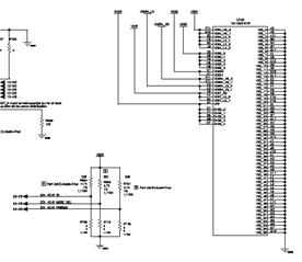
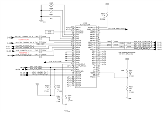
6.- Would you please review the schematic implementation for accuracy.
  • Hi Alonso,

    I'm still looking into this and will share feedback shortly.

    Best,

    Lucas

  • Hi Alonso,

    My apologies for the delay.

    1.  MODE_SEL should be pulled low. Will auto-negotiation occur with the TLK and its partner? This will determine how ST should be strapped.

    2. PRBSEN should be pulled low for normal operation. I recommend including a pull-up resistor footprint so you have the option to pull PRBSEN high for PRBS testing.

    3. I recommend pulling PRTAD[4:0] low for default port address setting, assuming there is no other device on your MDIO network with the same address. Note that the PHY address field on the MDIO protocol (PA[4:1]) will need to match the PRTAD[4:1] pin value, and PA[0] will need to =0 for proper register access.

    4. JTAG is optional and I recommend not using it. MDIO interface can be used for device configuration. TDI and TCK should be grounded when unused, while other pins can be left floating.

    5. Programming configuration is performed through MDIO. Here is a presentation which covers some programmable parameters. A register map is also provided in the datasheet.

    TLK10xxx SerDes Overview.pdf

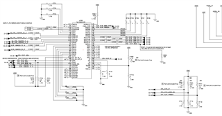
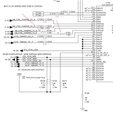
    6. Here is my feedback on your schematic. Note that you are still responsible for ensuring your design will work as intended.

    • HSTXAP/N: Please confirm signals are AC coupled.
    • HSRXAP/N: Looks good, AC coupled.
    • INA0P/N: Looks good, AC coupled.
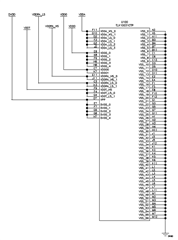
    • INA[3:1]P/N: Unused pins tied to GND with a shared 100-ohm resistor. Please use one 100-ohm resistor per P/N pair (3 resistors total). The purpose is to maintain 100-ohm differential impedance on each unused pair.
    • OUTA0P/N: Please confirm signals are AC coupled.
    • OUTA[3:1]P/N: Looks good, unused outputs left floating.
    • LOSA: Looks good, connected to controller device.
    • LS_OK_IN_A: Please pull this pin to VDDO with 50k resistor. I'm assuming this pin will be unused. This is the configuration used on the TLK10xxx EVM.
    • LS_OK_OUT_A: Looks good, unused output left floating.
    • PDTRXA_N: Looks good, pulled high for normal operation.
    • RSV[7:0]: Looks good, left floating.
    • REFCLK0P/N: Looks good, AC coupled, assuming the reference clock meets datasheet requirements.
    • REFCLK1P/N: Looks good, AC coupled, assuming the reference clock meets datasheet requirements.
    • CLKOUTAP/N: Connected to headers. These CML outputs must be AC coupled.
    • PRBSEN: Please pull low for normal operation. I recommend including a pull-up resistor footprint so you have the option to pull PRBSEN high for PRBS testing.
    • PRBS_PASS: Looks good, connected to controller device.
    • ST: Please pull high/low depending on use of auto-negotiation and MDIO clause. The safest design option is to include both pull-up and pull-down resistor footprints.
    • MODE_SEL: Please pull low for 1G-KX mode.
    • PRTAD[4:0]: I recommend pulling these pins low for default port address setting.
    • RESET_N: Looks good, connected to controller device. Note that RESET_N must be held asserted (low logic level) for at least 10us after device power stabilization.
    • MDC: A pull-up resistor is generally not required. Please double check with other devices on your MDIO network. It may be safer to keep a pull-up resistor footprint just in case.
    • MDIO: This signal must be externally pulled up to VDDO using a 2k resistor.
    • TDI: Unused. Please pull to GND.
    • TDO: Looks good, unused pin left floating.
    • TMS: Looks good, unused pin left floating.
    • TCK: Unused. Please pull to GND.
    • TRST_N: Looks good, unused pin left floating.
    • TESTEN: Looks good, pulled low. Pull-up resistor footprint included.
    • GPI[2:0]: Looks good, pulled low.
    • AMUX[1:0]: Looks good, left floating.
    • VDDA_LS/HS: Connected to 1.0V supply. Decoupling matches TLK10xxx EVM. I recommend using a 0-ohm resistor instead of a ferrite bead to match TLK10xxx EVM.
    • VDDT_LS/HS: Connected to 1.0V supply. Decoupling matches TLK10xxx EVM. I recommend using a 0-ohm resistor instead of a ferrite bead to match TLK10xxx EVM.
    • VDDD: Connected to 1.0V supply. Decoupling matches TLK10xxx EVM. I recommend using a 0-ohm resistor instead of a ferrite bead to match TLK10xxx EVM.
    • DVDD: Connected to 1.0V supply. Decoupling matches TLK10xxx EVM. I recommend using a 0-ohm resistor instead of a ferrite bead to match TLK10xxx EVM.
    • VDDRA_LS: Connected to 1.8V supply. Decoupling matches TLK10xxx EVM. I recommend using a 0-ohm resistor instead of a ferrite bead to match TLK10xxx EVM.
    • VDDRA_HS: Connected to 1.8V supply. Decoupling matches TLK10xxx EVM. I recommend using a 0-ohm resistor instead of a ferrite bead to match TLK10xxx EVM.
    • VDDO[1:0]: Connected to 1.8V supply. Decoupling matches TLK10xxx EVM. I recommend using a 0-ohm resistor instead of a ferrite bead to match TLK10xxx EVM.
    • VPP: Looks good, tied to DVDD.
    • VSS: Looks good, tied to GND.

    Best,

    Lucas

  • Hi Lucas,


    I really appreciate all the detailed feedback that you have provided, it really helped. I emailed you the updated schematic based on your feedback, would you please review and confirmed I've implemented all of the feedback provided?

     Thanks;

     Alonso

  • Hi Alonso,

    I haven't received an updated schematic. If you're having trouble sending it to me directly, you can also send it to your FAE and he will share it with me for review.

    Best,

    Lucas

  • Here you go.

  • Hi Alonso,

    Here are my comments on your updated schematic.

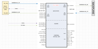
    • HSTXAP/N: Looks good, assuming AC coupling is added on another sheet.
    • INA[3:1]P/N: My apologies, upon closer inspection I realized my original recommendation here was incorrect. The datasheet states "Unused CML differential input pins should be tied to ground through a shared 100-ohm resistor." The purpose of this is to force unused inputs into a known state (logic 0), not to maintain 100-ohm differential impedance. I recommend using your original design, where all pins are tied together and pulled to GND through a single 100-ohm resistor.
    • OUTA0P/N: Looks good, assuming AC coupling is added on another sheet.
    • LS_OK_IN_A: Looks good, 50k pull-up to VDDO.
    • CLKOUTAP/N: Looks good, AC coupling added.
    • PRBSEN: Looks good, pulled low for normal operation. Pull-up resistor footprint and connection to controller device included for design flexibility.
    • ST: Looks good, pulled low for Clause 45 operation. Pull-up resistor footprint and connection to controller device included for design flexibility.
    • MODE_SEL: Looks good, pulled low for operation with auto-negotiation. Pull-up resistor footprint and connection to controller device included for design flexibility.
    • PRTAD[4:0]: Looks good, all pulled low for default port address setting.
    • MDC: Looks good, assuming 4.7k pull-up to VDDO is needed by other devices on MDIO network.
    • MDIO: Looks good, 2.2k pull-up to VDDO.
    • TDI/TCK: Looks good, tied to GND.
    • Power supply pins: I don't see supply networks included in this image, however these recommendations I made are not critical.

    Best,

    Lucas

  • Hi Lucas,

    Thanks for the feedback, I've a question. This is a VPX board that will connect to a chassis with other VPX boards. I don't have visibility to the other boards, I understand that the HSTXAP/HSTXAN are not showing the AC-coupling caps as they should be on the Receiver side. Is there any harm if I add 0402 Zero-ohm resistors just in case the AC-Coupling caps are not present on the receiving device. I.e. if the Receiving board don't have the AC coupling caps present, I can change the Zero-ohm resistors for caps, but if they are present, I can leave the Zero-ohm resistors. Would this cause any signal integrity or performance issues?

    Updated schematics and Power Supply pins below

  • Hi Alonso,

    There is no harm including an 0402 footprint on differential traces for AC coupling/0-ohm resistor. I recommend moving forward with this design so you have the flexibility to add/remove AC coupling, depending on what's included on the other board.

    Best,

    Lucas

  • Great, thanks for all of your support Lucas.

  • No problem.

    Best,

    Lucas