Part Number: TUSB1104
Tool/software:
Dear Sir/Madam,
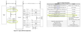
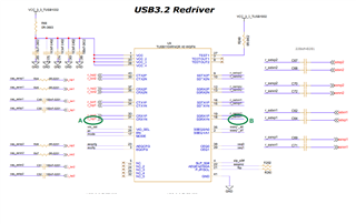
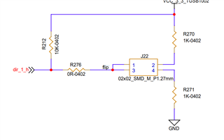
We have developed FMC card using TI Redriver TUSB1104 for our 10 Gbps, USB3.2, Gen2, 2x2 mode IP core testing. Host boards will be Xilinx, Altera, Lattice Semiconductor, Asmedia High speed FPGA host cards.
We need to clear USB compliance testing.
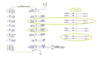
In pin strap mode we got below result:
Asmedia Type C port + Amphenol cable
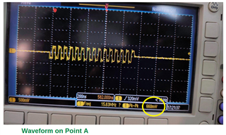
Lane1-> Not enumerate. Recovery during enumeration.
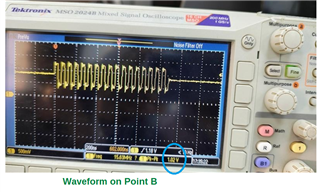
Lane2-> USB20 Enumeration
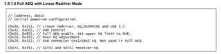
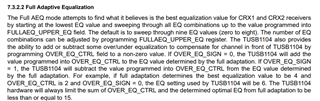
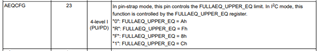
We are planning to go Malaysia for compliance testing on 27th Feb 2024.As per mentioned in datasheet, In Full Adaptive Equalization mode, TUSB1104 will automatically determine what it believes is the best equalization setting. In Full AEQ mode, the TUSB1104 will attempt to determine the best settings regardless if the channel is short, long, or somewhere in between. We are planning to use this mode.
So please guide us how to use this mode and how it works. Also please share application guide or procedure for using of Full AEQ mode.