Part Number: SN65DSI83
Tool/software:
I got PCB now and I can display Test pattern from SN65DSI83 now.
I connect 100MHz CLK to REF CLK pin now, and no MIPI-DSI CLK because source device is not ready.
I want output "27MHz" LVDS CLK.
In datasheet, I recognize that
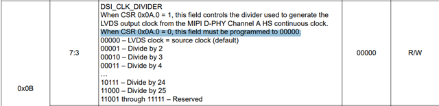
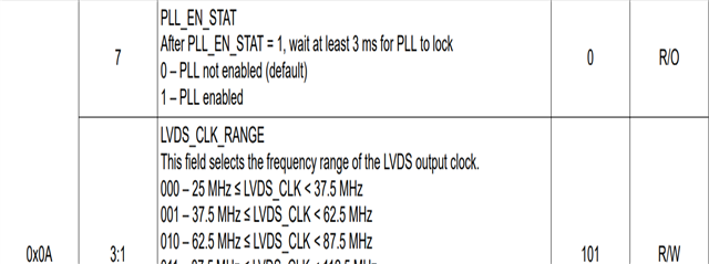
ADDR 0x0B 1:0 bit are the setting for changing FREQ from REFCLK to LVDS CLK
ADDR 0x0B 7:3 bit are the setting for changing FREQ from DSI CLK to LVDS CLK.
By the way
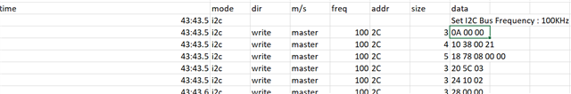
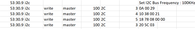
I set 0x0A =0x00 + 0x0B = 0x01, and next time I set 0x0A =0x00 + 0x0B = 0x2A,
LVDS CLK changed !
Why does it happen?