This thread has been locked.

If you have a related question, please click the "Ask a related question" button in the top right corner. The newly created question will be automatically linked to this question.

SN75DPHY440SS: function mode status

Part Number: SN75DPHY440SS

Tool/software:

hi TI team

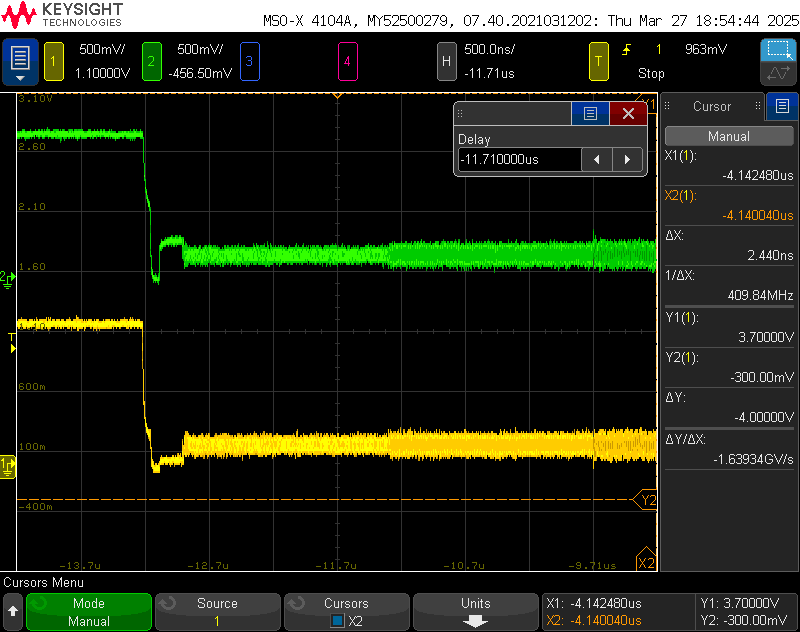
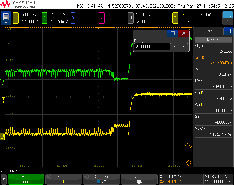
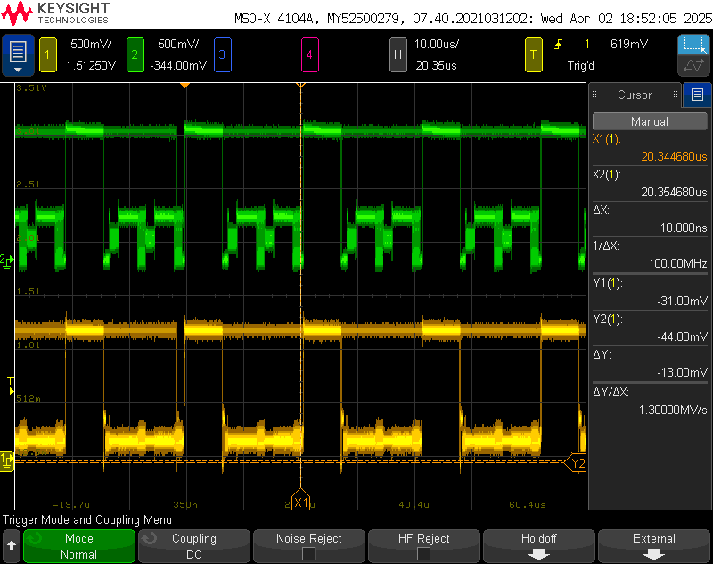
Does sn75dphy440ss has register indicate function mode status?

  • Hi,

    The DPHY440 does not have register that can indicate the different function mode status. Is there a specific issue you are facing?

    Thanks

    David

  • Hi David

    We meet some problem

    Host can't recognize MIPI signal from DPHY440

    if remove DPHY440 bypass signal ,function is OK

    Following are waveform 

    yellow means DPHY440 input(side A)

    green means DPHY440 output(side B)

    A.pin 10,MIPI CLK

    B.Date lane

  • Hi,

    Are you seeing the issue on both the data and the clock lane?

    Looking at the clock waveform, I don’t see the LP state.

    For both the data and clock, can you zoom into the waveform and verify there is a sequence of LP11-LP01-LP00 before transitioning to HS mode?

    Thanks

    David 

  • Hi David

    Here are waveform , MIPI source is DS90UB954 test pattern 

    CLK signal don't have LP mode, only 400MHz CLK 

    channel 0,1 and 3 seem NO HS data output at side B

    channel 0,1 waveform are similar 

    channel C and 2 output looks fine

    I will show 3 kind of waveform

    A. Channel 0,1

    B. Channel 3

    C. Channel C & 2

    yellow : Positive signal

    green : Negative signal

  • Channel 0&1 Side A

    Channel 0&1 Side B (seems NO video out)

  • Channel 3 ,side A (this channel is 954's CLK signal)

    Channel 3 ,side B

  • Channel C & 2 ,side A

    Side B

  • Hi Larson, 

    Can you provide a register dump of the UB954 along with your intiialization script for the device? 

    Have you tested setting the CSI-2 transmitter on the UB954 to non-continuous mode? This is set in register 0x33[1]. 

    Best,

    Zoe

  • Hi Zoe

    attach is register dump of UB954

    00: 60 00 1e 20 df 01 00 fe 1c 10 7a 7a ab 09 00 7f    `.? ??.???zz??.?
    10: 00 00 00 00 00 00 00 00 00 00 00 00 00 00 04 02    ..............??
    20: 20 01 00 00 00 00 00 00 00 00 00 00 00 00 00 00     ?..............
    30: 00 00 00 03 40 01 00 00 00 00 00 01 14 6f 00 40    ...?@?.....??o.@
    40: 00 e0 71 01 00 00 00 00 00 00 00 12 01 03 04 64    .?q?.......????d
    50: 00 00 00 03 00 00 00 00 5e 00 00 32 32 1c 6c 6e    ...?....^..22?ln
    60: 52 d0 6a 00 00 1c 6c 6e 52 d0 6a 00 00 78 88 88    R?j..?lnR?j..x??
    70: 2b 2c e4 02 dc 0f 30 c5 00 01 00 00 20 00 00 00    +,????0?.?.. ...
    80: 00 00 00 00 00 00 00 00 00 00 00 00 00 00 00 00    ................
    90: 00 00 00 00 00 00 00 00 00 00 00 00 00 00 00 00    ................
    a0: 02 0f 00 00 08 19 00 00 00 00 00 00 00 00 00 00    ??..??..........
    b0: 04 0e 20 08 25 00 18 00 88 33 83 74 80 00 00 00    ?? ?%.?.?3?t?...
    c0: 00 00 00 00 00 00 00 00 00 00 00 00 00 00 00 00    ................
    d0: 00 43 94 03 60 f0 01 00 00 00 00 00 00 00 00 00    .C??`??.........
    e0: 00 00 00 00 00 00 00 00 00 00 00 00 00 00 00 00    ................
    f0: 5f 55 42 39 35 34 00 00 00 00 00 00 00 00 00 00    _UB954..........

  • Hi Larson, 

    From this thread, it seems like non-continuous clock mode needs to be used for this application. This is changed by writing register 0x33=0x01 instead of 0x33=0x03 in your present initialization script. 

    Would you be able to repeat this testing and provide insight on results? 

    Best,

    Zoe

  • Hi Zoe

    set 0x33=0x01

    waveform :CLKN

    yellow :input / green :output

  • Hi Zoe

    I try another way ,change the input port of CLK of DPHY440SS

    954's CLK to 440SS's pin  5&6 

    CLK sine wave successfully output to DPHY440SS side B

    I guess maybe that was wrong at beginning

    CLK signal should connect to 440SS's pin 5&6 not pin 9&10

    (I change pin ordering because of layout reason)

    so I have a question 

    Does UB954 to 440SS (4 data + 1 CLK lanes) should follow the default pin of 440SS?  

    or doesn't, just only CLK  need? 

    Can 440SS auto detect the data lane order then adjust ?

    in UB954 datasheet P.24 ,data lane looks be in order

  • Hi,

    With DPHY440 being a MIPI re-timer, you have to connect the 954's CLK output to the DPHY440SS clock input. But the data lanes can be swapped as long as the lane order is matching between the input and the output of the DPHY440. 

    Please also note that unlike DSI, CSI-2 does not have a back channel path. But when using DPHY440 in a MIPI CSI-2 design, special attention must be paid to lane 0. With Lane 0 path (DA0P/N and DB0P/N) supporting bi-directional LP signaling, it is very important that DB0P/N LP TX is connected to an unterminated LP RX.  If DB0P/N LP TX is connected to a HS RX, then LP signaling will not be able to reach the LP11 levels and which will cause the DPHY440 to not enable HS data path on Lane0.

    Below is a workaround to disable LP and enable HS path on lane 0 only. Please note with LP being disabled, the source must send only HS data. 

    Enable HS path for Lane 0 only:

    Write Register 0x50 with 8’h01 //Override enable for HS TX path

    Write Register 0x51 with 8’h01 //HS TX path enabled.

    Write Register 0x61 with 8’h00  // Disable LP path.

    Write Register 0x70 with 8’h01  //Override enable for HS RX path

    Write Register 0x71 with 8’h01  // HS RX path enabled.


    Bit 0 is lane 0

    Thanks

    David

  • hi David

    you mean DPHY440 in a MIPI CSI-2 design

    lane 0 can't PASS LP and HS in a same time?

    so MIPI source must be only HS data in each lane 

  • Hi,

    In order to support DSI, DPHY440 lane 0 is different from all the other lanes as shown below.

    So you can see lane 0 has LP TX and RX at both input and output. Since it has both LP TX and RX, the DPHY440 lane 0 output expect to see an unterminated TX. Otherwise the DPHY440 will not able to transition from LP to HS mode.

    You can use I2C to disable LP and enable HS mode, and 954 must be configured to send HS data only. Below is the workaround.

    Below is a workaround to disable LP and enable HS path on lane 0 only. Please note with LP being disabled, the source must send only HS data. 

    Enable HS path for Lane 0 only:

    Write Register 0x50 with 8’h01 //Override enable for HS TX path

    Write Register 0x51 with 8’h01 //HS TX path enabled.

    Write Register 0x61 with 8’h00  // Disable LP path.

    Write Register 0x70 with 8’h01  //Override enable for HS RX path

    Write Register 0x71 with 8’h01  // HS RX path enabled.


    Bit 0 is lane 0

    The same approach can be used for other lanes as well if you want to disable LP and just transmit HS data.

    Thanks

    David

  • hi 

    I don't understand witch bit is for other lane in Register 0x50,0x51,0x61,0x70,0x71

    Could you provide an example?

    Thanks

  • Hi,

    To enable HS path for all lanes, please see below codes

    Write Register 0x50 with 8’h1F //Override enable for HS TX path

    Write Register 0x51 with 8’h1F //HS TX path enabled.

    Write Register 0x61 with 8’h00  // Disable LP path.
    Write Register 0x70 with 8’h1F  //Override enable for HS RX path
    Write Register 0x71 with 8’h1F  // HS RX path enabled.
    Thanks
    David