This thread has been locked.

If you have a related question, please click the "Ask a related question" button in the top right corner. The newly created question will be automatically linked to this question.

TCA9517-Q1: B-side controlled by MCU causing issues

Part Number: TCA9517-Q1
Other Parts Discussed in Thread: ISO1640, TCA9517, TCA9800,

Tool/software:

Hi All,

I am using the TCA9517ADGKR as a I2C repeater. This is needed because I am communicating with a I2C device that's not on the same board as the MCU.

Original Setup:
- VCCA and VCCB are 3.3V , the A-side is connected to the MCU with 1K pull-ups; 

- The B-side is connected to the ISO1640 with 1k pull-ups;

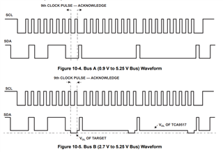
The problem is the typical value of VOL on the B-side of the TCA9517 is 0.52V and the maximum VIL of the ISO1640 is 0.480V. This doesn't work because the voltage doesn't get low enough for the ISO1640.


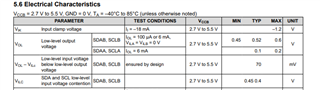
A solution was to swap what's connected to the A and B sides, because the A-side can go as low as 0.2V. 
Current setup:
-VCCA and VCCB are 3.3V , the A-side is now connected to the ISO1640 with 1K pull-ups; 

-The B-side is now connected to the MCU. 

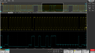
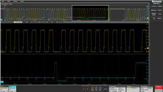
The new problem: After swapping the 2 sides, I am now seeing these "hitches" appear in the clock signal and the SDA have this "step" characteristic in the signal. Is this a byproduct of switching the sides? Why does this occur? 


  • The TCA9517's VOL is higher than that of all other devices connected to it to allow the buffer to detect whether the pin must currently behave as an input or an output. So different VOL levels, depending on which device is driving, are normal.

    The TCA9800/1/2/3 uses a different mechanism to detect the direction, which allows low VOL on both sides. But it has similar restrictions (B side must not be connected to the ISO1640), and you must not connect pull-ups on the B side.

  • Hi Akeem,

    These hitches or pedestals are normal operation for the TCA9517-Q1. 

    See figure 10-4 and Figure 10-5 of the TCA9517-Q1 datasheet on page 15 of 26: 

    I agree with Clemens, VOLB is a larger voltage (~0.52V) when driving a LOW from A-side to B-side. The input voltage on B-side = VILC = 400mV. The output is higher than its input in order to keep direction of the buffer from locking up. Therefore, when driving the reverse direction (B-side back to A-side) VIL = VILC = 400mV < VOLB = 0.52V. 

    Therefore, we get this step in the waveform which is normal. 

    Regards,

    Tyler 

    LINK to FAQ