This thread has been locked.

If you have a related question, please click the "Ask a related question" button in the top right corner. The newly created question will be automatically linked to this question.

DP83TG720EVM-MC: DP83TG720R-Q1 SPE Testing – Mode 1 & Mode 4 Issues, Comparison with CRB

Other Parts Discussed in Thread: DP83TG720EVM-MC, DP83TG720R-Q1

零件編號: DP83TG720EVM-MC

工具/軟體:

嗨,TI 團隊,

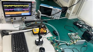
我們已經使用 TekExpress 成功設定了 SPE 測試環境,現在我們可以執行測試模式 1~7,如所附螢幕截圖 test environment.jpg 所示。

我們希望您能就模式 1 和模式 4 的一些失敗結果和問題提供協助。以下是我們的客製化專案板 (X303-EC) 和 CRB 參考板之間的比較:

模式 1 → 無波形輸出,無法進行測試。 CRB 也會出現此問題。

模式 2 → X303-EC 測試結果為失敗;CRB 測試結果為通過。然而,誤差幅度僅 ~0.02。

模式 4 → 無法測試。根據軟體 SOP,此測試需要特殊夾具。 CRB 也存在同樣的問題。

模式 5 → 結果失敗,與 CRB 相同。

模式 6 → 通過,結果與 CRB 相同。

我們將非常感謝您就以下事項提供指導:

  1. 模式 1 和模式 4 是否有任何已知問題或其他要求?

  2. 您能否確認在每種測試模式下波形擷取的正確偵測位置(例如,TRD_P/N或其他) ?

Test_Mode_1

begin

000D 0001
000E 0904
000D 4001
000E 2000

end

Test_Mode_2

begin

000D 0001
000E 0904
000D 4001
000E 4000

end

Test_Mode_4

begin

000D 0001
000E 0904
000D 4001
000E 8000

000D 001F
000E 0453
000D 401F
000E 0019

end

Test_Mode_5

begin

000D 0001
000E 0904
000D 4001
000E A000

end

Test_Mode_6

begin

000D 0001
000E 0904
000D 4001
000E C000

end

 CRB.pdfX303_EC_A_SPE_CN1.pdf

  • Hi Jim,

    这是国际 E2E 论坛。为了让我们队员看懂你的帖子,请用英文写,谢谢。

    (This is the international E2E forum. To allow our team members to understand your posts, please write in English, thanks).

    __________________

    The configuration of the DP83TG720 for compliance testing is described in an application note (https://www.ti.com/lit/an/snla371b/snla371b.pdf). After the power up of the DP83TG720, it must be programmed with the master or slave initialization script described in Section 3 to optimize the electrical performance - please perform this initialization if it is not already part of your procedure. Then after this, the test modes can be configured.

    > Mode 1 → No waveform output, no test possible. The CRB also has this issue.

    The notes from Section 4 regarding Test Mode 1 say that 1) there must be a link between the DP83TG720 and the link partner before running the test, and 2) the clock signal used for the test is exposed on the CLKOUT pin of the DP83TG720. Can you verify that there is a link partner, the link is up, and the CLKOUT signal from the PHY is being measured?

    > Mode 2 → X303-EC test result is fail; CRB test result is pass. However, the error magnitude is only ~0.02.

    Test mode 2 is used for the MDI jitter test. If it works on the TI board but the customer board has issues then likely the failure is related to some part of the layout design of the customer board. Since the failure is so marginal it could also be helpful to run the test several times or see if there is something that can be tightened/optimized in the test setup.

    > Mode 4 → Unable to test. This test requires special fixtures according to the software SOP. The same issue applies to CRB.

    OK, this sounds like a hardware limitation. I am not sure we can provide any advice to assist with this.

    > Mode 5 → Result failed, same as CRB.

    Test mode 5 is used for the power spectral density (PSD) test. One common reason for failing PSD is that there could be too much insertion loss between the PHY and the scope. If it is possible to shorten the cables or use fewer connector stages, it could help improve the test results. Otherwise, it is a matter of layout.

    > Mode 6 → Pass, the result is the same as CRB.

    OK.

    In general, I recommend that you review the PHY initialization and test procedures to make sure they are following our recommendations, then see if any improvements can be made to the test fixture. If there are still issues after this we can help you review the layout of the customer PCB.

    Best,

    Evan Su

  • TI Team,

    Thank you for your previous response regarding Test Mode 1 for the DP83TG720R-Q1.

    In your note, you mentioned that according to Section 4 of the application note, the test requires:

    1. A valid link between the DP83TG720 and a link partner

    2. The clock signal for the test is exposed on the CLKOUT pin

    We would like to confirm the following points:

    1. Does this mean that two PHY devices must be physically connected via SPE (TRD_P/N) and in a Link-Up state before Test Mode 1 will output the 125 MHz clock?

    2. Based on the datasheet, we believe that Pin 16 is the CLKOUT output . Could you please confirm this is the correct pin for observing the 125 MHz signal?

    3. Since Pin 16 is a single-ended output , and our oscilloscope setup currently uses a differential probe , what is the correct method to probe this signal?

      • Should one side of the probe be connected to Pin 16 and the other side to ground?

      • Or do you recommend using a single-ended probe for this measurement?

    Your clarification will help ensure we are performing the measurements correctly. Thanks in advance!

  • Hi Jim,

    Does this mean that two PHY devices must be physically connected via SPE (TRD_P/N) and in a Link-Up state before Test Mode 1 will output the 125 MHz clock?

    Yes.

    Based on the datasheet, we believe that Pin 16 is the CLKOUT output . Could you please confirm this is the correct pin for observing the 125 MHz signal?

    Pin 16 is the default CLKOUT pin, so unless CLKOUT has been purposefully reassigned to another pin (most likely you have not), the 125 MHz can be expected there.

    Since Pin 16 is a single-ended output , and our oscilloscope setup currently uses a differential probe , what is the correct method to probe this signal?

    On our boards we generally route CLKOUT to an SMA or similar cable connector. For a differential probe, I think the first option of connecting one side to Pin 16 and the other to GND should be OK to generate a viewable waveform. I am not sure about the possible test performance differences compared to a cable.

    Best,

    Evan Su

  • Hi Evan 

    During our Test Mode 1 validation, we connected two DP83TG720R-Q1 CRB boards together via SPE (TRD_P/N), configuring one as Master and the other as Slave.

    We observed the following:

    We connected a differential probe such that the positive input was attached to the Master board’s CLKOUT SMA (Pin 16), and the negative input to the Slave board’s CLKOUT SMA (Pin 16).

    Under this setup, we were able to observe a stable 125 MHz waveform on the oscilloscope, and the TekExpress Mode 1 test passed.

    Our question:
    We understand that CLKOUT is a single-ended signal. From a signal integrity and measurement accuracy perspective:

    Is this differential probing method (Master CLKOUT vs. Slave CLKOUT) a valid and recommended way to observe the clock in Test Mode 1?

    Or should the standard practice be to probe only one PHY's Pin 16 (e.g. Master) using a single-ended or pseudo-differential setup (as previously advised)?

    Would this differential measurement method introduce jitter masking, phase offset, or affect accuracy in any way?

    We would appreciate your insights regarding the validity and implications of this probing method.

    Best regards,

    jim shen

    CRB mode1 pass

  • Hi Jim,

    Is this differential probing method (Master CLKOUT vs. Slave CLKOUT) a valid and recommended way to observe the clock in Test Mode 1?

    According to page 20 of the OA 1000BASE-T1 PMA test suite overview (https://opensig.org/wp-content/uploads/2024/01/1000BASE-T1-PMA-Test-Suite-1-3-v1-2.pdf), the transmitter timing jitter test has 3 cases. Case 1 and Case 2 use Test Mode 1 and are run on a DUT in either master mode or slave mode and the clock is routed from the DUT to the oscilloscope. The method you described where each differential line in a differential probe is connected to a different device is not supported.

    Or should the standard practice be to probe only one PHY's Pin 16 (e.g. Master) using a single-ended or pseudo-differential setup (as previously advised)?

    This would be in compliance with the specification.

    Would this differential measurement method introduce jitter masking, phase offset, or affect accuracy in any way?

    I have not tested your method before but going from principles, I don't see positive effects or understand the motivation from mixing two single-ended clocks from different devices into one differential signal for measurement. The master and slave clocks are not the same, even in theory, because the test description separates the master transmitter timing measurement from the slave transmitter timing measurement. When a test is run, only one PHY is supposed to be the DUT, and is configured to either master or slave mode for a measurement. In such tests that require a link partner, the link partner not a DUT. So the composite differential clock you are describing would have double the normally expected swing, likely worse jitter/phase characteristics, and in my understanding is not the quantity the test is intended to measure.

    Best,

    Evan Su