This thread has been locked.

If you have a related question, please click the "Ask a related question" button in the top right corner. The newly created question will be automatically linked to this question.

TUSB212: TUSB212IRWBR adjust USB2 Eye diagram issue

Part Number: TUSB212

Tool/software:

Hi, TI support teams,

We are using TI/TUSB212IRWBR of our design.

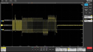
We meet to USB2 yes diagram fail issue and would like to adjust the USB2 signal driving strength by TI/TUSB212IRWBR.

1.We did below testing:

(1)Our original schematic design: DC_BOOST/ENA_HS be high. ( The stronggest driving strength.)

(2)We remove TI/TUSB212IRWBR and measurement it again.

There is no difference of item(1) and Item(2). Please refer attached pdf file.

2.The D1 and D2 of TI/TUSB212IRWBR. Which one is for Host side? Which one is for device side?

We checked the spec of TI/TUSB212IRWBR. The page 1 of spec is D2 for Host and D1 for device. The page10,12 of spec is D1 for Host and D2 for device. It seems not consistant.

Please also refer the attached file.

3.It seems TI/TUSB212IRWBR no working.

We also attached our schematic design of the pdf file.

Could you help to double check our schematic design again?(Actually we already provide our full sch to TI FAE reviewed.)

TI-TUSB212IRWBR_20250711.pdf

Thank you.

  • Hello,

    (1)Our original schematic design: DC_BOOST/ENA_HS be high. ( The stronggest driving strength.)

    (2)We remove TI/TUSB212IRWBR and measurement it again.

    There is no difference of item(1) and Item(2). Please refer attached pdf file.

    Can you monitor the ENA_HS and CD pins? These should be able to help debug whether or not your redriver is enabling or not. My guess is that currently, the redriver is not enabling, which may be due to the sequencing of your testing. The TUSB212 must be powered and out of reset before any signals are sent through the USB2 trace. If not, the redriver will not enable, which will cause the signal to not be boosted.

    For the DC_BOOST/EQ pins, we recommend starting lower, like at level 0/1 for EQ and Mid for DC_BOOST, as setting these settings too high in systems of shorter lengths can cause over-compensation.

    2.The D1 and D2 of TI/TUSB212IRWBR. Which one is for Host side? Which one is for device side?

    We checked the spec of TI/TUSB212IRWBR. The page 1 of spec is D2 for Host and D1 for device. The page10,12 of spec is D1 for Host and D2 for device. It seems not consistant.

    Please also refer the attached file.

    The TUSB212 is bidirectional, there is no host or device side. It is able to boost the signal that moves under it regardless of the direction of the signal.

    3.It seems TI/TUSB212IRWBR no working.

    We also attached our schematic design of the pdf file.

    Could you help to double check our schematic design again?(Actually we already provide our full sch to TI FAE reviewed.)

    My only remark on the schematic would be to lower EQ to ensure overcompensation is not an issue at the start. Also, just to confirm, the DP/DM lanes are connected beneath the redriver, correct?

    Thanks,

    Ryan

  • Hi Marx,

    I am marking this thread as resolved due to inactivity. If you have any questions or need more assistance, feel free to reply here.

    Thanks,

    Ryan