


Part Number: DP83867IR
Tool/software:
Hi all,
I saw E2E below.
I understand that it is necessary to be satisfied power-off sequence for three-supply.
When My customer checked the power-off on the actual machine, the waveform shown below is shown.
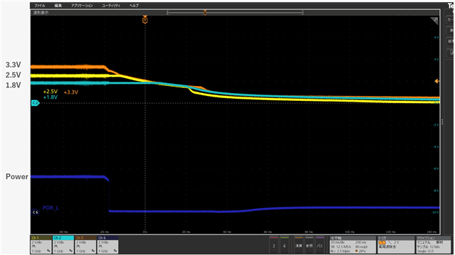
The power down of 1.8 V and 2.5 V is not exactly simultaneous, but does it cause a problem?
The E2E mentioned that there is an in-chip diode, but my customer's schematics has this diode on the LDO line on their board.(Like below)
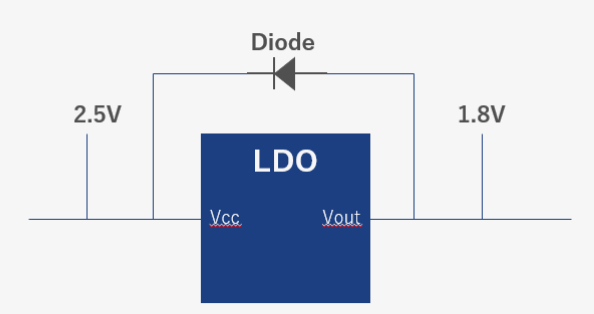
The purpose is to flow the residual charge of 1.8V to 2.5V when the power is turned off. The current flowing through the diode is very small because only the residual charge is lost.
The reason that the potential of 1.8V is higher than that of 2.5V is due to the forward voltage (Vf) of the diode, and they believe that the diode is operating as intended.
If this diode is connected, I believe that there will be no problem even if the power down does not occur at the same time as shown in the waveform. Is it correct?
I would appreciate your opinion.
Best Regards
Ryusuke
