This thread has been locked.

If you have a related question, please click the "Ask a related question" button in the top right corner. The newly created question will be automatically linked to this question.

DP83867IS: Design review

Guru 11040 points
Part Number: DP83867IS

Tool/software:

Hello,

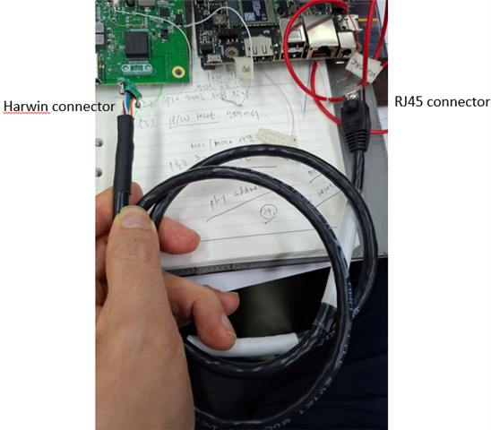
My customer wants to use DP83867IS in conjunction with NVIDIA Jetson AGX Orin's SOM.

They have an issue with the RGMII interface not working between the DP83867IS and the NVIDIA SOC.

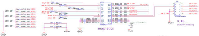
Q1. Please review the circuit design below to see if there are any problems.

CD.pdf

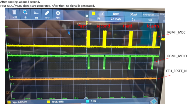
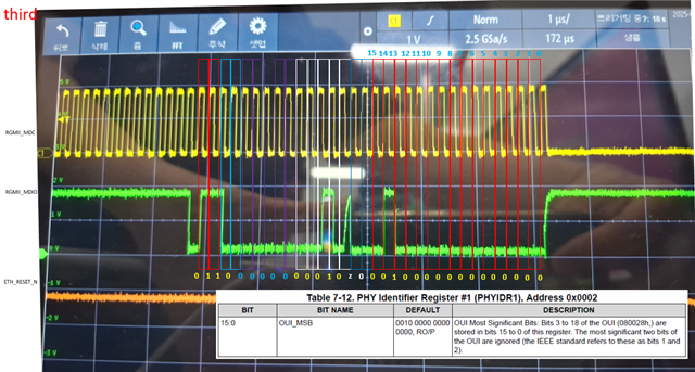
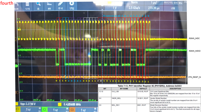
Q2. The files below are images capturing the power sequence and clock signal of the DP83867IS.

       Q2-1. Referring to the second image on page 1, the output of the XI signal is output about 85mS after the 1.0V power supply is stabilized. It seems that the clock output is too late. Could this cause a problem in the operation of the DP83867IS? (Please refer to the clock signal output  on page 2)

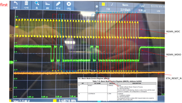
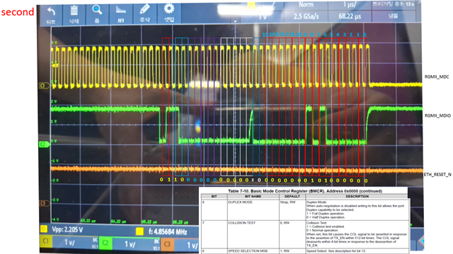
       Q2-2. Referring to the first image on page 3, they thought that the clock signal was output late because of the NVIDIA Reset signal, so they changed the reset signal to H/W reset. Are the resets they changed correct?

DP83867 power sequency and Clock output.pdf

Q3. Has DP83867IS been used with NVIDIA SOCs before? Please advise on this use case

Thank you.

JH

  • JH

    What specific issue are they seeing with the RGMII interface? Are they able to link up with the DP83867IS and its link partner? 

    When operating in three-supply mode, the 1.8V VDDA1P8 supply must be stable within 25ms of the 2.5V VDDA2P5 supply ramping up. There is no sequencing requirement for other supplies when operating in three supply mode.

    Thanks

    David

  • Hi David,

    Thank you for your reply.

    I asked the customer a detailed description of the issue symptoms.

    In the meantime, please review the customer's circuit and power, reset signal, clock output, etc. for any issues with timing, and then provide your opinion.

    For reference, regarding the VDDA1P8 power supply, you can check the stabilization time of the 1.8V power supply by referring to the first image of the DP83867 power sequence and clock output.pdf file shared above.

    BRs,

    JH

  • JH

    Looking at their schematic, I would recommend to enable Auto-Negotiation. This is done by putting RX_CTL into Mode 3 as shown below.

    Mode 3 means having a 5.76k pullup and a 2.49k pulldown.

    Can you also share the magnetics and RJ45 portion of the schematic?

    Thanks

    David

  • Hi David,

    Thank you for your review.

    I changed the strap_Configuration from mode4 to mode3. (RX_CTRL)

    And I share the magnetics and RJ45 portion of the schematic (below)

    BRs,

    Sungun Kim

  • JH

    I am looking at their RJ45 connector and it is not an RJ45 connector as shown below.

    Before we look at the RGMII side, are they able to link up with DP83867 link partner?

    Thanks

    David

  • Hi David,

    It is connected using a cable.

    And I share MDC and MDIO.

    1

    2

    3

    4

    [ test condition ]

    -- R35 open, H/W reset

    -- Strap Configuration: RX_CTRL is Mode3


    Thanks

    Best regards.

    Sungun Kim

  • JH

    Why are we looking at the Serial Management Interface? Do they now have issue over the Serial Management Interface? 

    We never validated the DP83867 with this Harwin connector, so I honestly don't know how the Harwin connector will impact the Ethernet signal integrity, and in turn, causing Ethernet link issue.

    Have they verified that they are able to link up with the DP83867 link partner? Can they please dump out the DP83867 register 0x0000 to 0x001F, 0x006E, and 0x006F?

    Thanks

    David