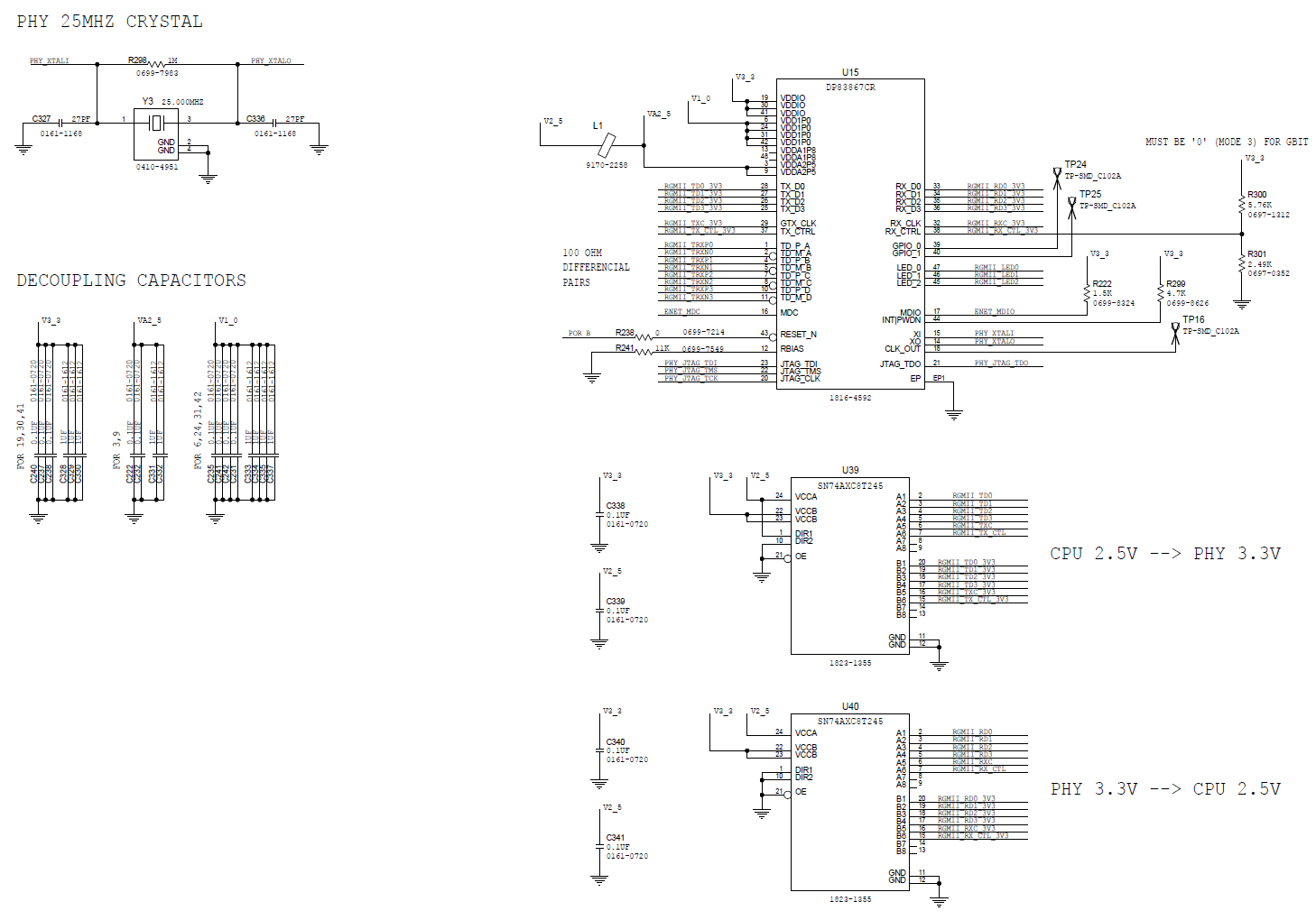
Part Number: DP83867CR
Tool/software:
I have modified a working design where I replaced a Marvel 88E1118R PHY with the TI DP83867CRRGZ PHY.
the PYH is located on a daughetboard with an i.MX6 Quad CPU and the RJ45 connector (MagJack V890-1AX1-A1) is on the motherboard.
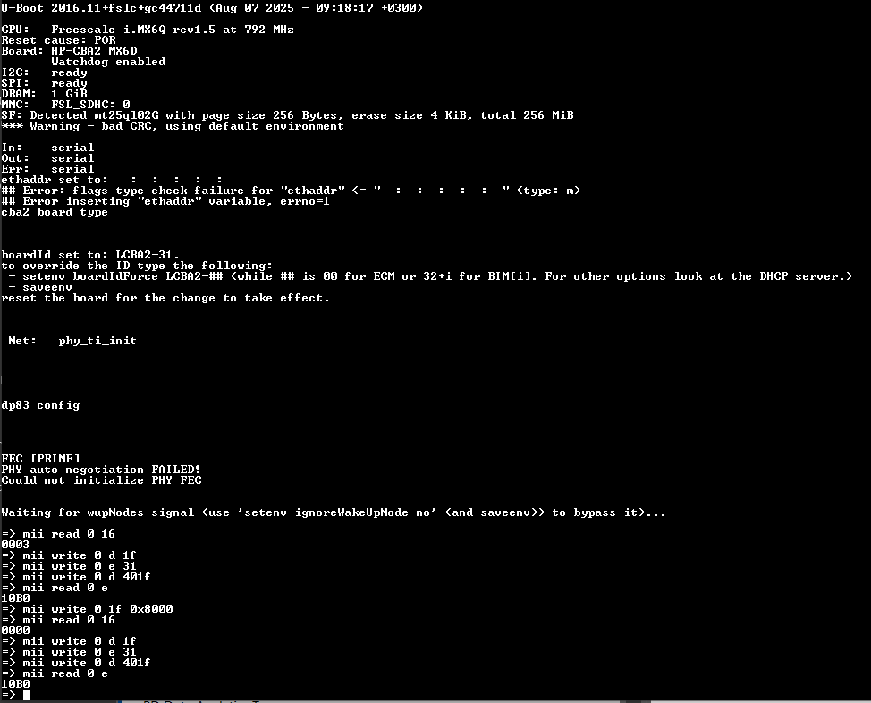
The MDIO/MDC interface is working fine at 250KHz (measured with scope) and the registers are:
=> mii read 0 0
1140
=> mii read 0 1
794D
=> mii read 0 2
2000
=> mii read 0 3
A231
=> mii read 0 4
01E1
=> mii read 0 5
0000
=> mii read 0 6
0064
=> mii read 0 7
2001
=> mii read 0 8
0000
=> mii read 0 9
0300
=> mii read 0 a
4000
=> mii read 0 b
0000
=> mii read 0 c
0000
=> mii read 0 d
0000
=> mii read 0 e
0000
=> mii read 0 f
3000
=> mii read 0 10
1012
=> mii read 0 11
0402
=> mii read 0 12
0000
=> mii read 0 13
0400
=> mii read 0 14
29C7
=> mii read 0 15
0000
=> mii read 0 16
0003
=> mii read 0 17
0040
=> mii read 0 18
6150
=> mii read 0 19
4000
=> mii read 0 1a
0002
=> mii read 0 1b
0000
=> mii read 0 1c
0000
=> mii read 0 1d
0000
=> mii read 0 1e
0002
=> mii read 0 1f
0000
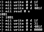
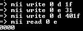
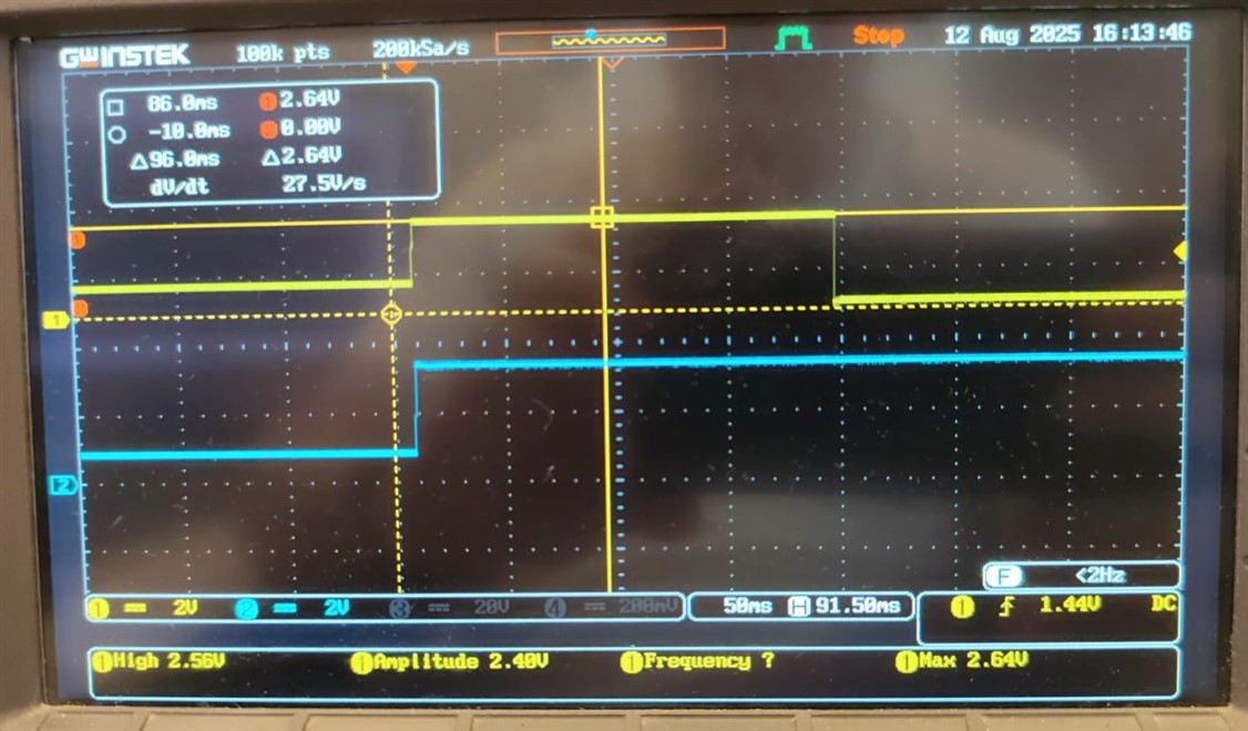
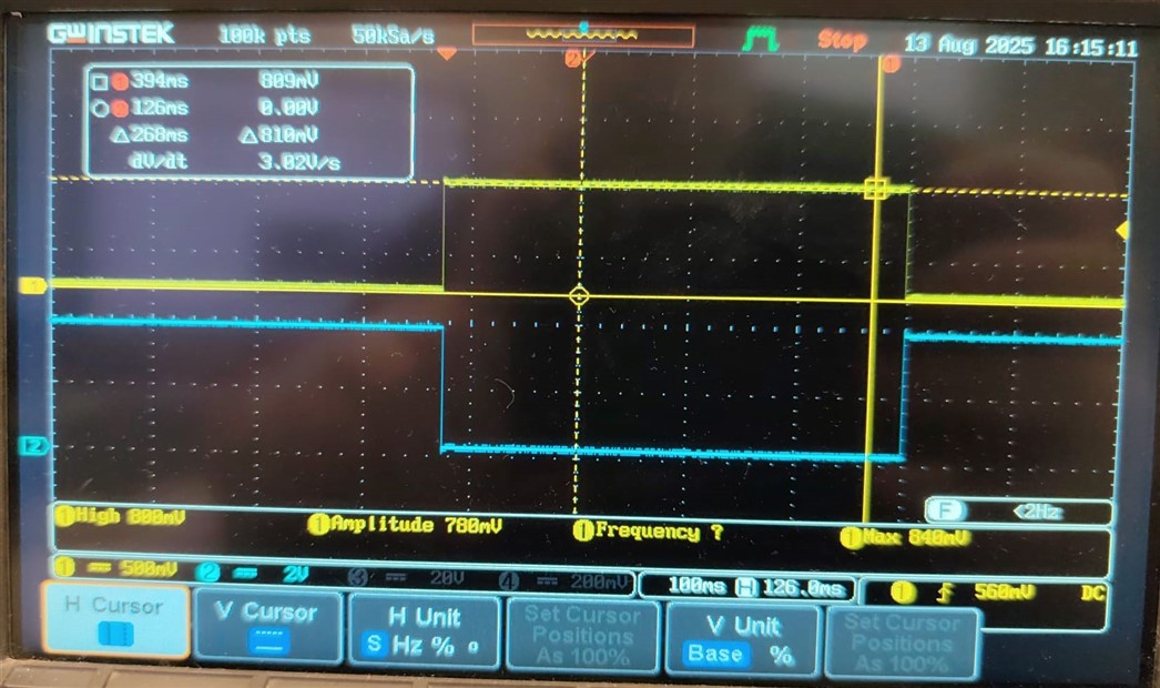
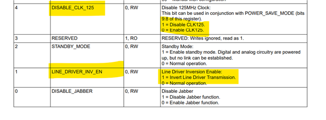
When I enable ('0') the DISABLE_CLK_125 bit (address 0x10 bit 4) I get a nice clock signals is this the same as CLK_O_DISABLE bit on register 0x0170?
By changing register 0x0170 I get 25MHz for default Reference Clock, 125MHz for transmit and recieve channels and 25Mhz for receieve channels divided by 5.
Are the recieve and transmit clocks on the CLK_OUT pin derived from the RX_CLK and TX_CLK of the MAC interface? or are they internally generated?
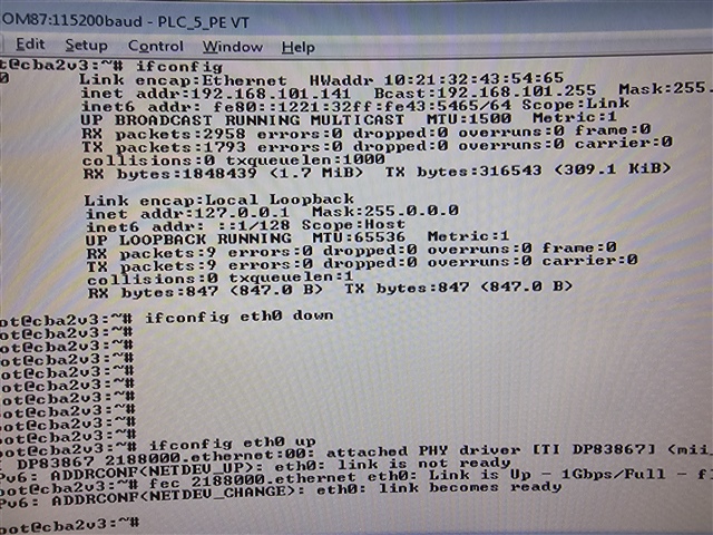
What is causing the LINK to be up although no cable is connected?
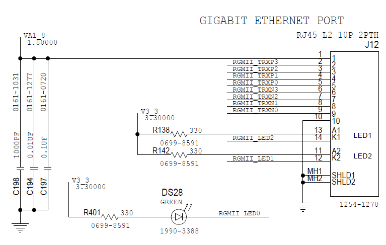
The daughterboards schematics
The motherboards schematics - Disregard the 1.8V to the tap it is floating (uninstalled resistor on another page) It was needed for the Marvell PHY.