SN65LVDS32: How to terminate SN65LVDS32 input pins for LOW output level when no input is connected

Part Number: SN65LVDS32
Other Parts Discussed in Thread: SN65LVDS31

Tool/software:

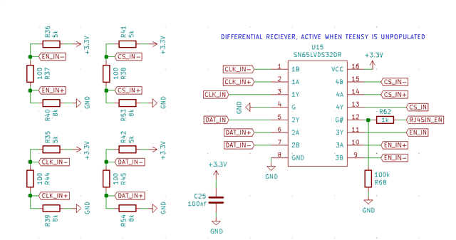
Hi, I am using the SN65LVDS32 for a design for handling CAT5 data signals. With my current schematic the pins are left in an unpredictable state when no signal is being sent into the CAT5 input jack. 

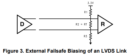
This is my current schematic, with a 100 ohm hysteresis resistor across the differential inputs and both + and - signals biased to ground by 10k resistors:


I find with CAT5 signal coming in from an SN65LVDS31 this schematic works for me. 

But when nothing is plugged in some of the outputs are high and some are low, seemingly at random. 

When no differential signal is being received I need all the outputs to go low. What do I need to change to accomplish this?

Please advise.

  • Looking at something like this where the - inputs are biased high and the + inputs are biased low by default leading to a LOW output:


    Please confirm if this is the correct approach for default LOW output and will work with my application receiving signal from SN65LVDS31.

  • Hi Emmett,

    The VID needs to be below -100mV to output low. With this circuit, the VID will be 0V, so you will be in an undetermined state. You will need to remove the pulldown resistor on the B pins and replace it with a pullup to Vcc. You will also need to modify the resistance value of the pulldown on the A pins to be . Similar to the below schematic except R1 is a pulldown to GND and R3 is a pullup to Vcc. The pullup resistor on the B pins will need to be lower resistance than the pulldown on the A pin to achieve a negative voltage across RT. You can star with a pullup value of 4.99k Ohms and a pulldown value of 8k Ohms.

    However, if you refer to AN-1194 Failsafe Biasing of LVDS Interfaces (Rev. C), the current from the failsafe network needs to be to lower the resistance of both resistors while keeping the same ratio to increase the current if you are operating in a very nosy environment. You may need to experiment with these values some to figure out what the sweet spot is based on the noise that will be present. 

    Also, this seems like the same circuit we were discussing in this thread, so be sure to modify the G and /G connections accordingly (+) SN65LVDS32: SN65LVDS32DR G̅ Pin Not Deactivating Chip Outputs - Interface forum - Interface - TI E2E support forums

    regards,

    matt 

  • Okay so would this schematic work?

    R1 = 5K pull-ups on B, R3 = 8K pulldowns on A, R2 = 100 ohm hysteresis across.

    How should the value R2 be chosen in relation to R1 and R3?

  • Hi Emmet,

    That's correct. R2 is the standard 100Ohm resistor defined by the TIA-644 standard for LVDS. 

    One last thought here: As I mentioned in my last reply, this will significantly reduce your noise margin and distort your signals when the driver is on because of the differential voltage offset. If you remove the pullup/pulldown resistors form the bus and utilize the internal failsafe feature in the device, it will give you much better noise immunity and it won't offset anything on the lines. However, the failsafe output will be high. One way to work around this is by inverting the logic by adding NOT gates on the single-ended TTL input and output pins of the driver/receivers. This would give you the best performance for what you're trying to achieve. 

    Regards,

    Matt