Part Number: SN75DP139
I am developing a DP++ to HDMI retimer circuit using the SN75DP139RSBR. I have been looking at the EVAL schematic for the SN75DP139 and it appears that there is flexibility on the lane assignments as well as the polarity of the lanes.
For the Sink Side (HDMI) this is not a huge factor since i am just puting pads on the board for the HDMI wires to solder onto so i can place them in a way to mitigate crossing the differential pairs.
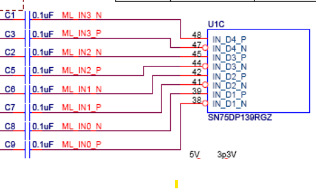
For the Source Side (mini DP++) this is getting tricky. The screenshot below shows the EVAL schematic.
First question, Can i have P-->P instead of N --> P (as the eval does)?
Second question, the Eval Board D3 (connector)-->D4 (SN75DP139), D2 (connector)-->D3 (SN75DP139), D1 (connector)-->D2 (SN75DP139), D0 (connector)-->D1 (SN75DP139). Is this flexible in that i can reaarange the data pairs going into different pair inputs of the SN75DP139?