This thread has been locked.

If you have a related question, please click the "Ask a related question" button in the top right corner. The newly created question will be automatically linked to this question.

TCAN4551-Q1: how is the TCAN4551-Q1 performance?

Part Number: TCAN4551-Q1
Other Parts Discussed in Thread: TCAN4550

Now we integrate the TCAN4551 drvier plugin(1.6.0), but we found received one CanFD(2M) message will spend 311us and send on need 200us in the ISR processing. the SPI rate is 10M, the MCU main clock is 350M. currently the  performance not match the requirements.  Any performance information about this controller?  

eg: Send or receive one Can/CANFD message, how long time will spend?


i check the recveive sequece.

i found there are 6 step about spi process.

1> read IR register

2>clear IR regiser.

3>get the newData flag.

4>get the CANID and datalength

5>get the data.

6>clear the new data flag.

Any way to quick the  process? 


  • Hello Haitao,

    Making the SPI communication as efficient as possible by reducing idle time between SPI Read/Write transactions, and to use multi-word SPI Read/Write transactions whenever possible such as when reading the message data contained in consecutive address cells will reduce the number of SPI bits transferred by reducing the need for an address field for every 32-bit data word in a single-word SPI Read/Write transaction.  This will help minimize the total time needed to communicate across SPI and minimize the CAN FD message process time.

    There is no procedural fix to the overall process that could shorten the number of steps to send or receive a CAN FD Message, with the TCAN4551-Q1 device, so improving the efficiency of every step is all the options we have.   

    However, we do have a new device in development that will include Direct Memory Access improvements specifically to address the overall efficiency for the exact reasons you are asking.  Samples of this device are targeted for March 2026, so depending on your design cycle, a more efficient option should exist later this year for you to consider.

    Regards,

    Jonathan

  • Is the new device available now? What is the specific part number, and is it hardware-compatible with the TCAN4551-Q1?

  • Hello Roy,

    No, as I previously stated, the new device is not available at the moment, and preliminary samples are targeted for March 2026. I won't put the new part number on this public forum until it has been added to the TI.com so I'll just refer to it as TCAN45xx for this conversation.

    TCAN45xx is built off of the TCAN4551-Q1 from a register map with the intent of being software compatible, but there are some additional registers and features being added to register addresses that are currently Reserved or Unused in the TCAN4551-Q1.  It does not share the same package or pinout as the TCAN4551-Q1 so any applications currently using the TCAN4551-Q1 would need a PCB revision to support the new TCAN45xx device. 

    Regards,

    Jonathan

  • Will the new device also be an SPI-to-CAN device?
    How does the new device improve efficiency, and between which components does the DMA operate?

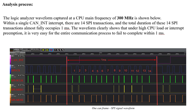
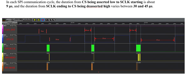
    We are currently using the TCAN4551-Q1. With this device, receiving a single standard CAN frame actually requires 14 SPI transactions. In addition, there is a noticeable amount of latency both before the SPI transfer starts and after the transfer ends, as shown in the waveform captured below.

    These delays cannot be resolved on the host MCU side.

    Under these conditions, would using your new device provide any improvement with respect to this issue?

  • Hi Roy,

    The new MCAN DMA improvements are directly intended to reduce the number of SPI transactions needed to send or receive a CAN message.  The new functionality allows reading and writing from known addresses to shift CAN messages into or out of the internal MRAM elements.  The nWKRQ pin can also be re-purposed to be a dedicated "new message" interrupt output which further eliminates the need for a read of the interrupt register followed by a write to clear.  

    So the current process to read a message out of MRAM for a RX FIFO 0 would be:

    1. Read IR register, see MCAN bit is set.
    2. Read MCAN IR register, see RX0N is set (new message in RX FIFO 0).
    3. Read RXF0S to see how many messages are in the FIFO, and what the start address is.
    4. If the base address in MRAM is not stored, read RXF0C to determine the base address
    5. Do the math to determine the FIFO address. Read the contents of the FIFO from MRAM
    6. Acknowledge the FIFO message by writing to RXF0A.

    An example process to read from the new RX DMA is:

    1. Detect that the nWKRQ pin (in new message interrupt mode) is pulled low.
    2. MCU reads a full FIFO element word of data from the RX DMA address (which is fixed and always the same)
    3. Check if the nWKRQ is still low.  If so, repeat step 2 until the nWKRQ pin goes high.

    This results in a single SPI read instead of 6+ reads being needed for every incoming message.

    There is also a RX DMA address for RX FIFO 1.

    Messages are also loaded into the TX FIFO through a dedicated TX DMA address in a similar fashion.

    However, the device will still support the older method used in the TCAN4550/1 devices for compatibility.

    I hope this address your question.

    Regards,

    Jonathan

  • Hi Jonathan,

    We have a few questions and would appreciate your clarification.

    1、Compared with the TCAN4551-Q1, approximately how much efficiency improvement can the new device provide? Are there any quantitative or measurable metrics available?

    2、We are currently using the nWKRQ pin for system wake-up from sleep. If the wake-up function is required, can the new device still be used, and if so, are there any limitations or trade-offs?

    3、Can the current Linux driver for TCAN4551-Q1 be directly compatible with the RX DMA mechanism of the new device? Will your team provide or complete the Linux driver adaptation for the new device?

  • Hi Roy,

    1、Compared with the TCAN4551-Q1, approximately how much efficiency improvement can the new device provide? Are there any quantitative or measurable metrics available?

    I don't have any quantitative or measurable metrics for this device and it is still in the development and validation phase.  However, as I previously noted, you will simply need to read the message data from the dedicated RX DMA Address allowing you to eliminate 6 or more SPI reads per message.  

    2、We are currently using the nWKRQ pin for system wake-up from sleep. If the wake-up function is required, can the new device still be used, and if so, are there any limitations or trade-offs?

    First off the new device will not be in the same package as the TCAN4550/1 devices and therefore it has a different pinout as well.  You would need to create or modify a board to accommodate the new device once it is available.  You don't need to use the nWKRQ pin as a new message interrupt and you could still use the other interrupt method to detect a new message has arrived, but this would require a read to the interrupt register making it less efficient.

    However, because there are no CAN messages being received during Sleep Mode, it may be possible to re-configure the nWKRQ pin to the default sleep wake interrupt function prior to placing the device into sleep mode.  Then after the device has woken up, you could re-configure it back to a new message interrupt as part of your re-initialization sequence.  This is just a thought.

    3、Can the current Linux driver for TCAN4551-Q1 be directly compatible with the RX DMA mechanism of the new device? Will your team provide or complete the Linux driver adaptation for the new device?

    I don't know if the current TCAN4x5x Linux driver supports the new features of this upcoming device.  I would think it would need some form of update, but I don't have any information to provide on that at this time.

    Regards,

    Jonathan