SN65DSI84: SN65DSI84: Device tree on MTK G510

Part Number: SN65DSI84
Other Parts Discussed in Thread: DSI-TUNER

We are using the SN65DSI840Q1 chip as a bridge from MIPI to LVDS on MTK Genio-510.

However, it's not working properly, so we need some help to check if the device tree is incorrect. 


display_overlay.dts

/dts-v1/;
/plugin/;

#include <dt-bindings/pinctrl/mediatek,mt8188-pinfunc.h>
#include <dt-bindings/interrupt-controller/irq.h>
#include <dt-bindings/gpio/gpio.h>

/ {
	fragment@0 {
		target = <&i2c5>;
		__overlay__ {
			 sn65dsi84: sn65dsi84@2d {
				compatible = "ti,sn65dsi84";
				reg = <0x2d>;
				enable-gpios = <&pio 11 GPIO_ACTIVE_HIGH>;
				// interrupts-extended = <&pio 6 IRQ_TYPE_LEVEL_LOW>;
				pinctrl-names = "default";
				pinctrl-0 = <&sn65_pins>;

				ports {
					#address-cells = <1>;
					#size-cells = <0>;

					port@0 {
						reg = <0>;

						sn65_dsi_in: endpoint {
							remote-endpoint = <&dsi0_out>;
							data-lanes = <0 1 2>;
						};
					};

					port@2 {
						reg = <2>;

						bridge_out_a: endpoint {
							remote-endpoint = <&panel_in_a>;
						};
					};

					port@3 {
						reg = <3>;

						bridge_out_b: endpoint {
							remote-endpoint = <&panel_in_b>;
						};
					};
				};
			};
		};
	};

	fragment@1 {
		target = <&dsi0>;
		__overlay__ {
			panel@0 {
				status = "disabled";
			};
			
			/delete-node/ ports;
			ports {
				port {
					dsi0_out: endpoint {
						remote-endpoint = <&sn65_dsi_in>;
						data-lanes = <0 1 2>;
					};
				};
			};
		};
	};

	fragment@2{
		target = <&lcm1_tp_avdd>;
		__overlay__ {
			status = "disabled";
		};
	};

	fragment@3 {
		target = <&i2c0>;
		__overlay__ {
			touchscreen@5d {
				status = "disabled";
			};
		};
	};

	fragment@4 {
		target = <&dpi1>;
		__overlay__ {
			status = "disabled";
		};
	};

	fragment@5 {
		target = <&hdmi0>;
		__overlay__ {
			status = "disabled";
		};
	};

	fragment@6 {
		target = <&hdmi_phy>;
		__overlay__ {
			status = "disabled";
		};
	};

	fragment@7 {
		target = <&cec>;
		__overlay__ {
			status = "disabled";
		};
	};

	fragment@8 {
		target = <&sound>;
		__overlay__ {
			dai-link-1 { /* HDMI */
				status = "disabled";
			};

			dai-link-2 { /* DPTX */
				status = "disabled";
			};
		};
	};

	fragment@9 {
		target = <&backlight_lcd0>;
		__overlay__ {
			status = "okay";
			default-on;
			power-supply = <&edp_panel_fixed_3v3>;
			enable-active-high;
		};
	};

	fragment@10 {
		target = <&disp_pwm0>;
		__overlay__ {
			status = "okay";
			pinctrl-names = "default";
			pinctrl-0 = <&disp_pwm0_pin_default>;
		};
	};
	
	fragment@11 {
		target = <&pio>;
		__overlay__ {
			disp_pwm0_pin_default: disp-pwm0-pin-default {
				pins1 {
					pinmux = <PINMUX_GPIO29__FUNC_O_DISP_PWM0>;
				};
			};

			sn65_pins: sn65-pins {
				sn65_en: pin-en {
					pinmux = <PINMUX_GPIO11__FUNC_B_GPIO11>;
					output-high;
				};
			};

			lvds_bk_en_high: lvds-bk-en-high {
				pins2 {
					pinmux = <PINMUX_GPIO8__FUNC_B_GPIO8>;
					output-high;
				};
			};
		};
	};
	
	fragment@12 {
		target-path = "/";
		__overlay__ {
			panel_lvds: panel-lvds {
				compatible = "panel-lvds";
				power-supply = <&edp_panel_fixed_3v3>;
				backlight = <&backlight_lcd0>;
				status = "okay";

				width-mm = <344>;
				height-mm = <193>;
				data-mapping = "vesa-24";
				dual-link;

				panel-timing {
					clock-frequency = <74250000>;
					hactive = <1920>;
					vactive = <1080>;
					hback-porch = <148>;
					hfront-porch = <88>;
					vback-porch = <36>;
					vfront-porch = <4>;
					hsync-len = <44>;
					vsync-len = <5>;
				};

				ports {
					#address-cells = <1>;
					#size-cells = <0>;

					port@0 {
						reg = <0>;

						dual-lvds-odd-pixels;
						panel_in_a: endpoint {
							remote-endpoint = <&bridge_out_a>;
						};
					};

					port@1 {
						reg = <1>;

						dual-lvds-even-pixels;
						panel_in_b: endpoint {
							remote-endpoint = <&bridge_out_b>;
						};
					};
				};
			};
		};
	};

	fragment@13 {
		target = <&edp_panel_fixed_3v3>;
		__overlay__ {
			regulator-state-mem {
				regulator-on-in-suspend;
			};
		};
	};
};


After applying the display_overlay on the board we got the follow dmesg, althrough the SN65DSI84 driver is probed.

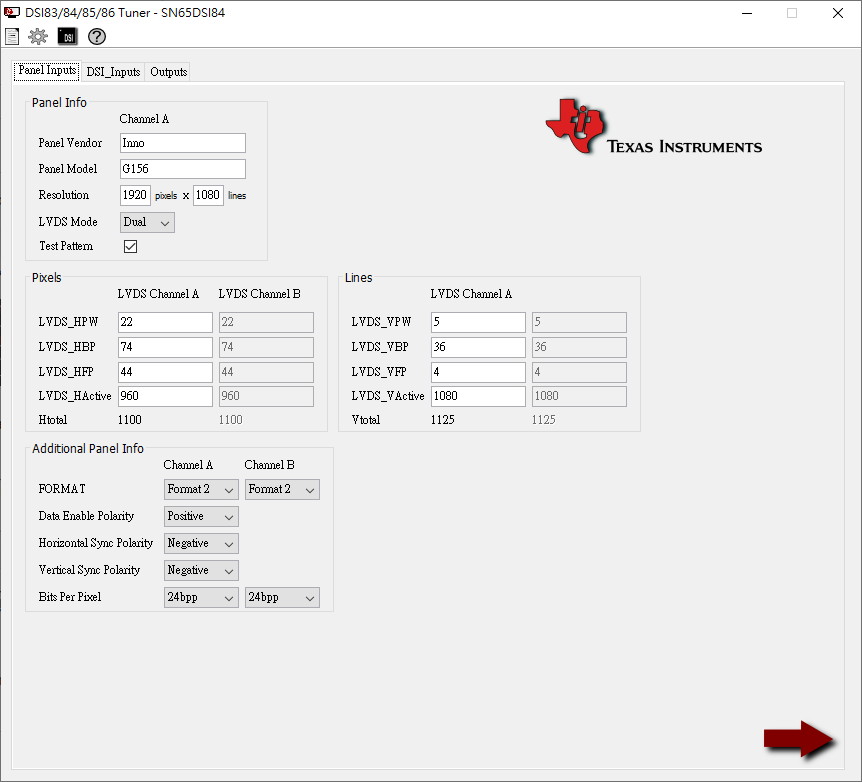
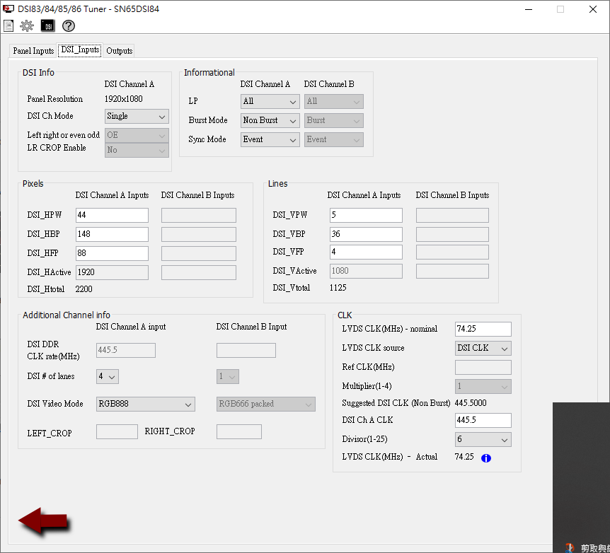
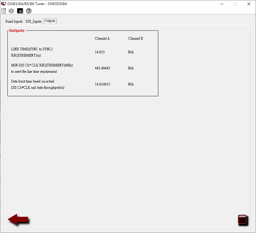
We tried to output the test pattern and set the DSI-TUNER value as below. After getting the CSR values, we tested CSR values using i2ctranfer command to write the register but it still output nothing.

image.png

image.pngimage.png

  • Hi Alan,

    I am not familiar with this device tree. Could you please share where you got this from.

    As a first step, we recommend using the test pattern generation. After programming the CSR registers, was there valid output on the LVDS output channel? You can check by probing the LVDS clock and data lanes and checking the clock frequency. Please also check register 0xE5 for any errors.

    Since this is using the DSI clock as a source, is the clock being programmed to the correct frequency? The clock should also be set in HS state as mentioned in the datasheet initialization and power-up sequence.

    Best regards,
    Ikram

  • Sorry, this didn't resolve my issue, I clicked by accident.

    This device tree follow the overlay of g510 sample code display-dsi2lvds.dts & reference from the following links.

    SN65DSI84: SN65DSI84 : with Raspberry Pi CM4S + AUO P370IVN02.2 – Test pattern works, but no video output - Interface forum - Interface - TI E2E support forums


    For the test pattern generation, can I directly change the CSR register using the I2C command like i2ctransfer ?

    Does it need some initialization process ?

    For example:

    i2ctransfer -f -y 5 w2@0x2d 0x09 0x00
    i2ctransfer -f -y 5 w2@0x2d 0x0A 0x05
    i2ctransfer -f -y 5 w2@0x2d 0x0B 0x28
    i2ctransfer -f -y 5 w2@0x2d 0x0D 0x00
    i2ctransfer -f -y 5 w2@0x2d 0x10 0x26
    i2ctransfer -f -y 5 w2@0x2d 0x11 0x00
    i2ctransfer -f -y 5 w2@0x2d 0x12 0x59
    i2ctransfer -f -y 5 w2@0x2d 0x13 0x00
    i2ctransfer -f -y 5 w2@0x2d 0x18 0x6c
    i2ctransfer -f -y 5 w2@0x2d 0x19 0x00
    i2ctransfer -f -y 5 w2@0x2d 0x1A 0x03
    i2ctransfer -f -y 5 w2@0x2d 0x1B 0x00
    i2ctransfer -f -y 5 w2@0x2d 0x20 0xc0
    i2ctransfer -f -y 5 w2@0x2d 0x21 0x03
    i2ctransfer -f -y 5 w2@0x2d 0x22 0x00
    i2ctransfer -f -y 5 w2@0x2d 0x23 0x00
    i2ctransfer -f -y 5 w2@0x2d 0x24 0x38
    i2ctransfer -f -y 5 w2@0x2d 0x25 0x04
    i2ctransfer -f -y 5 w2@0x2d 0x26 0x00
    i2ctransfer -f -y 5 w2@0x2d 0x27 0x00
    i2ctransfer -f -y 5 w2@0x2d 0x28 0x21
    i2ctransfer -f -y 5 w2@0x2d 0x29 0x00
    i2ctransfer -f -y 5 w2@0x2d 0x2A 0x00
    i2ctransfer -f -y 5 w2@0x2d 0x2B 0x00
    i2ctransfer -f -y 5 w2@0x2d 0x2C 0x16
    i2ctransfer -f -y 5 w2@0x2d 0x2D 0x00
    i2ctransfer -f -y 5 w2@0x2d 0x2E 0x00
    i2ctransfer -f -y 5 w2@0x2d 0x2F 0x00
    i2ctransfer -f -y 5 w2@0x2d 0x30 0x05
    i2ctransfer -f -y 5 w2@0x2d 0x31 0x00
    i2ctransfer -f -y 5 w2@0x2d 0x32 0x00
    i2ctransfer -f -y 5 w2@0x2d 0x33 0x00
    i2ctransfer -f -y 5 w2@0x2d 0x34 0x4a
    i2ctransfer -f -y 5 w2@0x2d 0x35 0x00
    i2ctransfer -f -y 5 w2@0x2d 0x36 0x24
    i2ctransfer -f -y 5 w2@0x2d 0x37 0x00
    i2ctransfer -f -y 5 w2@0x2d 0x38 0x2c
    i2ctransfer -f -y 5 w2@0x2d 0x39 0x00
    i2ctransfer -f -y 5 w2@0x2d 0x3A 0x04
    i2ctransfer -f -y 5 w2@0x2d 0x3B 0x00
    i2ctransfer -f -y 5 w2@0x2d 0x3C 0x10
    i2ctransfer -f -y 5 w2@0x2d 0x3D 0x00
    i2ctransfer -f -y 5 w2@0x2d 0x3E 0x00

  • Hi Alan,

    You can use the output from the DSI Tuner GUI to get a list of register writes required. 

    Guide for reference: https://www.ti.com/lit/an/slla332b/slla332b.pdf
    The outputs, as shown in "Control and Status Registers" section, will be a list of CSR register writes to program with these timings and configurations. 

    You can write to these registers via I2C. Please ensure that the clock source selections, frequency, etc and timings are accurate for the panel.


    Best regards,
    Ikram

  • Hi Ikram,

    I did generate the CSR list from DSI Tuner GUI as the example I pasted. Is the example commands correct for writing the registers via I2C?

    I'm using the InnoLux G156HCE-L01 Full-HD LVDS, could you please help to generate the test pattern with correct timing for the panel on DSI Tuner?

  • Hi Alan,

    You entries for the test pattern generation looks correct. Was there any output on display? You could also check the frequency on the LVDS clock output after running this.

    Since this is using DSI clock as reference, please make sure that the SoC is sending DSI clock at the correct rate: 445.5 MHz as you calculated. The DSI clock should be in HS mode. Please check the 0xE5 register after running this.

    Best regards,
    Ikram

  • Due to there is nothing display on the screen after writing the resigter of test pattern, is there any way to generate the test pattern without clock from DSI?

  • Hi Alan,

    When testing this when there is no display, was DSI clock enabled in HS state and working at the required frequency?

    As an alternative to DSI clock, you can also use the REFCLK as DSI source. For this, you would need to set the 0xA register for clock source and then set the multiplier to meet the LVDS clock frequency. Do you have a REFCLK connected to this device on the board? Please check the frequency of the REFCLK.

    The programming for the REFCLK can also be entered on the DSI tuner GUI, by setting LVDS clock source to REFCLK (instead of DSI CLK) and setting the multiplier to meet the display LVDS clock frequency.

    Best regards,
    Ikram