This thread has been locked.

If you have a related question, please click the "Ask a related question" button in the top right corner. The newly created question will be automatically linked to this question.

TCA9800: ICCB when EN is low

Part Number: TCA9800
Other Parts Discussed in Thread: TCA39306, LSF0102, TS5A23166, LSF0002

Hello all,

I'm evaluating the TCA9800 for an application where a I2C master device may lose power, but one of its slaves will continue to operate on battery power. I want to ensure the slave's I2C lines remain high when the master is not powered, and that the loss of master power does not cause excessive quiescent current to drain the battery.

I bought a few samples of TCA9800 because it looked like a good fit. Master is on the A side, slave is on the B side. SCLA and SDAA have 5.6K pullups to VCCA, and there are no pullups on the B side. See attached diagram.

TCA9800 example.png

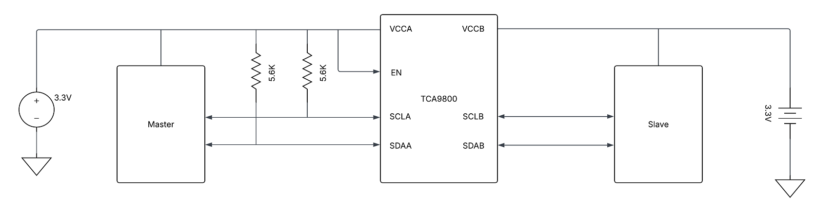
Everything seems to work as expected when power is applied on both sides and EN is high. When idle (SDA and SCL both high), ICCB is about 22uA, in line with the datasheet specs.

However, if I remove the VCCA power source, I see that ICCB increases to about 102uA. The datasheet does not seem to explicitly mention ICC specs when EN is low, but I had expected it to be no higher than when EN is high. In this state, I verified that VCCA, EN, SCLA, and SDAA are near zero volts. SCLB and SDAB are both at VCCB. ICCB seems to be passing entirely through the TCA9800 to GND.

Is this expected behavior? Is there some other part I should use which doesn't have this issue?

Regards,

Mike

  • I have no explanation, but try connecting the B side to the master.

  • Hi Mike,

    I will need more time to respond. Thanks. 

    Regards,

    Tyler

  • Hi Clemens,

    I did give this a try, but the repeater did not function properly. I'm guessing this is because I have pullups on the master side (I cannot change this), and the TCA9800 datasheet warns that external pullups on the B side is problematic.

  • Hi Mike,

    We are still looking into this and will update shortly.

    Regards,

    Jack

  • Hi Mike,

    I will need till noon tomorrow to answer your question. 

    Regards,

    Tyler

  • Hi Mike,

    Measuring ICCB while VCCA = 0V is not a case that was characterized in the datasheet.

    I assume that when VCCA = 0V and VCCB = ON, there is some circuitry that is keeping the device in a high-z state that is using some current which is why we see the jump to 102 uA. 

    For I2C buffers, I wouldn't be able to offer you a replacement that will have lower current in this state. 

    My question to is do you need buffer? If high-z is what you need, you can get the same effect with a passive level translator such as TCA39306, LSF0102. When these devices are EN = LOW, VCCA = 0V, I am more confident that the current through VCCB will still be very small since the internal architecture of these level shifters are simple passFETs. 

    if you do switch to a level shifter, you will not get the benefits of re-driving I2C (buffering) in your system. 

    See section 8.1.5. switch configuration - TCA39306

    Using 

    Regards,

    Tyler

  • Hi Tyler,

    In my case I do not need a buffer/repeater, the I2C bus is fully contained on one PCB and there's only one slave on the battery-powered side. And all slaves are fine with 3.3V so I don't need level translating either.

    A passive switch should work fine, though I want to ensure that the two sides are totally isolated when (both signal and power) when either side looses power. The problem is there are so many different options for passive switches, and figuring out if they offer the isolation I want requires digging into each datasheet, which is very tedious.

    I found the TCA9800 via this previous thread, but other parts with "powered-off protection" or "power-off isolation" were mentioned as well. Maybe those terms refer to the isolation feature I want. Does the TCA39306 offer that as well?

    Regards,

    Mike

  • TS5A23166/7

  • Thanks Clemens,

    Looking at the datasheet, it's not clear to what extent the signals are isolated when the TS5A23166 is powered off.

    Others have reported unexpected leakage with these parts:

     TS5A23166: Voltage at VCC when NO powered but VCC disconnected 

     TS5A23166: Device Power Off characteristics 

     TS5A23166: No high impedance with floating VCC( Isolation in Powered-Down Mode vs Power off Protection) 

    So it seems that "Isolation in Powered-Down Mode, V+ = 0" needs to be taken literally, V+ needs to be zero volts for the isolation to happen. No spec on how close to zero volts is enough. But that's impossible to guarantee since the leakage current itself may pull V+ up a bit....

  • Hello Mike,

    Our Apps team is current out of office because of a US holiday. Please expect delays in our response. Thank you for your understanding.

    Regards,

    Josh

  • Hi Mike,

    "Isolation in Powered-Down Mode, V+ = 0" needs to be taken literally, V+ needs to be zero volts for the isolation to happen

    I agree with this statement. If you expect V+ to float, then you cannot ensure powered off impedance of the device. 

    This same idea applies to LSF0102. If the EN pin is not 0V, then high-z is not a guarantee. 

    Is there anyway you can use LSF0102 in switch mode, and ensure EN = 0V when VCCA loses power? 

    Regards,

    Tyler

  • Hi Tyler, sorry I was out of office all last week.

    Regarding the LSF0102, I don't think it fits my application. When sides A and B are both powered, both will be 3.3V. The LSF0102 datasheet states that for Vref_B should be higher than Vref_A by at least 0.8V for proper operation. I think using the LSF0102 would result in the A side signals (on the slave side, I guess) being clamped to 2.5V, which is not okay. Maybe additional pullup resistors on the A side would help...?

    And it's not clear from the LSF0102 datasheet what the expected leakage currents would be on the A side when the B side is powered down.

  • Hi Mike,

    The LSF0102 can be used in switch mode, where VREF_A = VREF_B. 

    If EN = 3.3V or 0V, there is no clamp to 2.5V. 

    LSF0002 could also work. What puts the LSF0102 or LSF0002 in high-z is when the EN = 0V.

    The leakage spec is defined in IIH, for when the input voltage is 5V, and VEN = 0V 

    Would <5.0uA leakage work for your design? 

    Regards,

    Tyler

  • Hi Tyler,

    5uA would be plenty low enough for me.

    But it's not clear if that IIH spec is valid for when Vref_A and/or Vref_B are unpowered (either zero or near zero volts). And does IIH apply to the Vref pins as well?

    How close to 0V does EN actually need to be in order for these specs to be valid? There is no way for me to guarantee the master-side supply voltage drops to exactly 0V when not powered.

    Overall I'm not clear on the proper way to use the LSF0102 in my application, for example whether the slave should be on the A or B side, how to drive the EN pin, etc.

    Maybe this is a reasonable way to do it, with both Vref pins biased by the master side supply? But the question remains as to whether EN will drop low enough to isolate the signals when the master side is unpowered. Need a spec on that.

  • Hi Mike,

    We do not spec the leakage for EN voltages that are non zero. I suspect that even EN = 0.1, 0.2... could lead to increased leakage but unsure by how much since it is not spec'ed. 

    The internal device is a pass FET

    So if the gate voltage which is tied to the EN pin is non-zero, there might be increased leakage between the input and output. 

    Is there an extra gpio pin on the slave that could be used to set EN = GND when the A-side supply is powered off? 

    Would you be open to using LSF0002? On the enable pin, you can bias to 3.3V for A-side supply. You could tie a 100k pulldown resistor from EN to GND. The difficult part is that when VCCA is powered on, there is a 33 uA leakage to GND in that case, but you can ensure powered off leakage this way. I assume you could size the pull-down resistor to always be at GND level. Even a 200k resistor would work. The PD resistor does not have to be incredibly strong. 200k PD would make 3.3V / 200k = 16.5 uA. Is this an option?

    Regards,

    Tyler

  • Hi Tyler,

    We do not spec the leakage for EN voltages that are non zero. I suspect that even EN = 0.1, 0.2... could lead to increased leakage but unsure by how much since it is not spec'ed.

    It's honestly baffling to me that this is an acceptable way to characterize a part. It's like an opamp which only provides specs at one exact supply voltage, or one exact temperature. Though it looks like the Nexperia datasheet also has the same issue...

    An aside question, are the LSF010x devices symmetric? The datasheet suggests always connecting EN to Vref_B with the bias network, but I don't see why flipping it to the Vref_A side wouldn't work exactly the same way.

    I have ordered some LSF0102 samples which will hopefully arrive today for testing.

    Would you be open to using LSF0002?

    No, mainly because of the tiny package.

  • Mike,

    We are still looking into this and will follow up shortly.

    Regards,

    Jack

  • Hi Mike,

    It's honestly baffling to me that this is an acceptable way to characterize a part. It's like an opamp which only provides specs at one exact supply voltage, or one exact temperature. Though it looks like the Nexperia datasheet also has the same issue...

    Note taken. 

    An aside question, are the LSF010x devices symmetric? The datasheet suggests always connecting EN to Vref_B with the bias network, but I don't see why flipping it to the Vref_A side wouldn't work exactly the same way.

    Yes they are symmetric. EN is connected to VREF_B for datasheet consistency. 

    Regards,

    Tyler