This thread has been locked.

If you have a related question, please click the "Ask a related question" button in the top right corner. The newly created question will be automatically linked to this question.

DS125DF1610: Retimer source clock 1.35GHz

Part Number: DS125DF1610

Hi Experts,

That at 675 MHz input, all channels can lock stably.
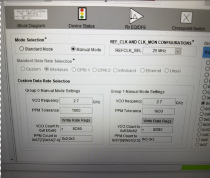
Our configuration uses a 675 MHz RX input, a 2.7 GHz VCO, and a 2.7 GHz retimer TX output. Right?

image.png

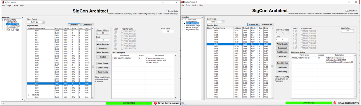
•We tried to program the user‑defined pattern (1010…) into registers 0x7C and 0x93, but the DSSC write operation was unsuccessful.
•After verifying the register map in the TI UI, we observed that both registers 0x7C and 0x93 are read‑only. We feedback this to TI, since their documentation indicates that these registers should be writable when using the user‑defined pattern feature.

SigCon:

image.png

  • Hi Che-Jung,

    I will check on this and will get back to you as soon as possible.

    Best regards,

    Greg

  • Hi Greg,

    Any findings so far?

    We attempted to source a 2.7 Gbps PRBS7 signal from the retimer TX port to our device.

    Our device requires a precise and stable 2.7 Gbps PRBS7 input to operate.

    However, the device is currently not functioning, and we suspect the issue may be related to instability in the retimer output.

    Our current retimer register configuration is as follows:

    • TX divider: 4
    • VCO frequency: 2.7 GHz
    • PRBS generator: PRBS7
    • Channel status: CDR locked

    Based on this configuration, we expect the retimer TX port to output a 2.7 Gbps PRBS signal. Could you please confirm whether this setup is correct for generating a 2.7 Gbps PRBS7 output, or if additional settings are required?

  • Hi Che-Jung,

    To clarify, is the device currently not outputting any PRBS signal at all? Or is the PRBS pattern not being acknowledged by the end point? Finally, are you utilizing the device PRBS generator to output PRBS7 from the retimer TX port?

    Best regards,

    Greg

  • Hi Greg,

    l've loop back retimer channel0 to channel 1 to used PRBS check check the signal is PRBS7. I have a question regarding the rate configuration:

    1. If I set the VCO to 10.8 GHz and configure Reg
      0x18 for a divide-by-4 ratio, the output should be 2.7 Gops, correct?
    2. Is it possible to set the VCO directly to 2.7 GHz, or must it remain within the 9.8-12.5 GHz range using the divider?

    I'm asking because our DUT is currently unable to detect the PRBS signal from the retimer. This makes me concerned about either the signal quality or a potential mismatch in the rate configuration.

    Could you help verify if my understanding of the VCO/divider setting is correct?

  •  Hi Che-Jung,

    1. Your understanding is correct.

    2. The VCO should remain within the 9.8-12.5 range.

    What are the writes you are using to configure the PRBS output? Please verify it follows the recommendations listed in this FAQ:

     [FAQ] DS125DF1610: How to setup the device to generate different PRBS pattern 

    Does your DUT have signal detect?

    Best regards,

    Greg

  • Hi Greg,

    We configured the registers via SMBus.

    We set the input clock to 675 MHz into the retimer RX, configured the VCO to 10.8 GHz, applied a ÷4 output divider, and then reset the CDR on all channels. With this configuration, the retimer outputs a 2.7 GHz PRBS signal.

    After that, I wrote Reg 0x7C = 0xAA and Reg 0x97 = 0xAA to source the user-defined pattern, intending to switch the retimer to output a 1.35 GHz clock.

    Our device detects a data rate of 2.63–2.688 Gbps on Channel 0 through Channel 15. We configured the PPM control registers as Reg 0x64 = 0x33 and Reg 0x67 = 0x00, so the expected frequency error should be approximately ±1000 ppm (0.1%). However, the measured data rate does not match our expectation.

    Additionally, on some channels, the output causes our device CDR to fail to lock at 2.7 Gbps. We ran the retimer (PRBS CHK) self-test on Channel 0 to Channel 15, and the HEO is around 0.96, which suggests the signal quality itself is good. Based on this, we suspect the issue may be related to a VCO frequency offset (output frequency shift) rather than signal integrity.

    Do you have any thoughts on this behavior? Is there any possibility that the VCO or clocking path could introduce an unexpected frequency shift under this configuration, or are there additional registers we should check?

    Please let me know if this configuration looks correct or if further adjustments are recommended.

    Best regards,
    Ron

  • Hi Ron,

    In addition to the settings you mentioned, did you configure register 0x1E, 0x09, and 0x30 for the user pattern generator? These are defined in the programming guide, here:

    Best regards,

    Greg

  • Hi Greg,

    Yes, I did configure register 0x1E, 0x09, and 0x30.

  • Hi Ron,

    Thanks for sharing the script. I will review it and respond with any comments this week.

    Best regards,

    Greg

  • Hi Ron,

    Additionally, on some channels, the output causes our device CDR to fail to lock at 2.7 Gbps. We ran the retimer (PRBS CHK) self-test on Channel 0 to Channel 15, and the HEO is around 0.96, which suggests the signal quality itself is good. Based on this, we suspect the issue may be related to a VCO frequency offset (output frequency shift) rather than signal integrity.

    Here, when you refer to "our device", what device does this indicate? Is this the DS125DF1610 or another device? Does the CDR remain locked on the TI retimer when a user pattern is configured?

    Best regards,

    Greg