This thread has been locked.

If you have a related question, please click the "Ask a related question" button in the top right corner. The newly created question will be automatically linked to this question.

TUSB211A-Q1: TUSB211A-Q1: USB2.0 compliance test?

Part Number: TUSB211A-Q1

Hi team,

This question is related to a topic I asked previously in the thread:
"TUSB211A-Q1: USB2.0 device side compliance test?"

Could you please help clarify this point again?

We understand that, in USB 2.0, the electrical physical layer compliance tests for both host and device are defined only for the transmitter (TX), and that there are no dedicated electrical tests defined for the receiver (RX). Therefore, we understand that receiver performance is typically validated through functional testing or interoperability testing.

However, what we would really like to understand is the reasoning behind this design philosophy.

Why does the USB 2.0 specification not define an electrical compliance test for the receiver side? In addition, could you please explain how receiver design margin is generally considered in USB 2.0?


Thank you,

Katsuya

  • Hi Katsuya-san,

    Why does the USB 2.0 specification not define an electrical compliance test for the receiver side? In addition, could you please explain how receiver design margin is generally considered in USB 2.0?

    Depending on if your designing a host or a peripheral, there are different tests that are needed.

    For a Host implementation, we typically are only concerned about the TX electrical tests and interoperability. A host application does not typically worry about the signal at the device side of a system, as outside factors that cannot be controlled like cable length or device design can have an impact on the overall signal that is not caused by the host. The USB2.0 electrical compliance spec outlines what tests are needed depending on if there are upstream or downstream ports, if you are receiving the signal, etc. 

    For a device/peripheral application, there are some specific tests related to receiver capabilities that are part of the test spec if it is a high speed peripheral. Section 3.2 and 3.3 of the test spec outline these tests. For a device application, these typically relate to any test specifying upstream port functionality.

    I would recommend looking through the electrical compliance spec to see what tests are outlined.

    Thanks,

    Ryan

  • Hi, Ryan

    Thank you for your response. I understand that some RX-related tests exist for high-speed peripherals in Sections 3.2 and 3.3.

    We also note that USB 3.0 includes dedicated RX compliance tests such as jitter tolerance and BER-based stress testing, which made us curious about why USB 2.0 does not follow a similar approach.

    My core question is about the underlying design philosophy of USB 2.0—specifically, who is responsible for ensuring that the receiver correctly receives a signal that is within spec at the receiver input.

    For example, even if some RX-related functional tests exist, they do not quantitatively characterize the receiver's electrical margin—such as sensitivity or jitter tolerance—in the way that TX compliance tests do. As a result, it seems possible that a device with marginal RX performance could pass all defined tests yet still fail in a real system when paired with a TX operating near its compliance boundary.

    Is it correct to say that USB 2.0 compliance testing assumes that a TX-compliant signal is generally expected to be receivable by a compliant RX? If so, what is the technical basis for that assumption?

    Thank you,

    Katsuya

  • Hi Katsuya-san,

    We also note that USB 3.0 includes dedicated RX compliance tests such as jitter tolerance and BER-based stress testing, which made us curious about why USB 2.0 does not follow a similar approach.

    This is likely due to the fact that the USB3 spec has data lanes dedicated to receiving the signal (RX lane), while the USB2 spec is a bidirectional channel, which I believe would place more-emphasis on a devices ability to transmit data rather than receive it. There is no TX or RX in the USB2 spec, only the bidirectional channel with a host and device in the system.

    For a USB3.0 application, due to the much higher data rate and different use cases (I.E DP alt-mode), there is a greater emphasis on the ability to ensure that a sink-side application is able to receive data without causing signal integrity issues.

    My core question is about the underlying design philosophy of USB 2.0—specifically, who is responsible for ensuring that the receiver correctly receives a signal that is within spec at the receiver input.

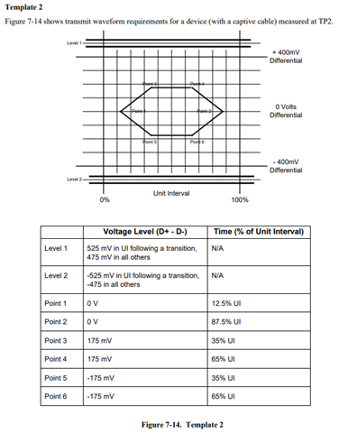
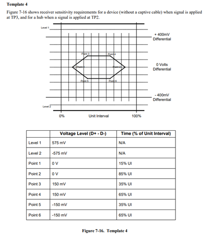
    There are two sides to a system, the host and the device. The host is in charge of ensuring that the signal it is transmitting is compliant to the eye diagram template 1 listed in section 7.1.2.2, while a device is in charge of ensuring the signal it is receiving meets either eye mask template 1 or 2 from the same section of the USB2 spec.

    I would recommend reading the USB2 Electrical Compliance Specification in conjunction with the USB2 Specification for a better understanding of what is expected from a host and the device.

    Is it correct to say that USB 2.0 compliance testing assumes that a TX-compliant signal is generally expected to be receivable by a compliant RX? If so, what is the technical basis for that assumption?

    I would recommend reading section 7 or section 10 of the USB2 specification to gain a better understanding of what is expected from the host, device, USB driver, and USB receiver. These are decisions that were not made by TI, but instead but the USB-IF organization. If a more theoretical or technical answer is needed, it may be good to reach out to them as well.

    Thanks,

    Ryan

  • Hi Katsuya,

    USB2 does not have a standardized way to force a Host or Device to respond to packet errors, so there is no way to perform the same type of receiver testing done in USB3.x.  USB2 compliance testing focuses mainly on signal quality tests with the understanding that if the transmitter can produce a clean signal the receiver is assumed to be robust enough.  The transmitter tests combined with the receiver sensitivity test ensures the device can operate in a noisy environment.

    Regards,

    Undrea

  • Hi Ryan, Undrea,

    Thank you both for the helpful explanations.

    From your responses, I understand that USB 2.0 compliance testing mainly focuses on transmitter signal quality, and that interoperability and receiver sensitivity tests are used to help verify that devices can operate in a system environment.

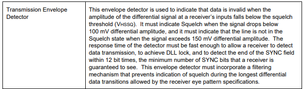
    One point I would like to understand more clearly is the purpose of the receiver sensitivity test (EL_16 and EL_17) . If the design philosophy assumes that a TX-compliant signal, combined with the specified channel conditions (such as cable characteristics), should result in a receivable signal at the receiver input, what role does the receiver sensitivity test play in the overall compliance framework?

    In other words, is it intended mainly as a safeguard to ensure a minimum RX capability, rather than to characterize the receiver's electrical margin in detail?

    I would appreciate any clarification on how the receiver sensitivity requirement fits into the overall USB 2.0 design philosophy.

    Thank you,

    Katsuya

  • Hi Katsuya-san,

    One point I would like to understand more clearly is the purpose of the receiver sensitivity test (EL_16 and EL_17) . If the design philosophy assumes that a TX-compliant signal, combined with the specified channel conditions (such as cable characteristics), should result in a receivable signal at the receiver input, what role does the receiver sensitivity test play in the overall compliance framework?

    In other words, is it intended mainly as a safeguard to ensure a minimum RX capability, rather than to characterize the receiver's electrical margin in detail?

    I believe you're understanding here is correct. EL_16 and EL_17 are used to ensure that any differential signal below 100mV is not misinterpreted as a valid transmission or packet and thus squelched, while also ensuring that any differential signal over 150mV is not immediately squelched and is instead treated as a valid transmission.

    If you look at page 136 of the USB2 spec, you can see that USB2 signals can be as low as 150mV and still be compliant to the USB 2 spec.

    EL_16 and EL_17 help to ensure the signals being received are being measured as expected and that the device is acting as expected as well.

    Thanks,

    Ryan

  • Hi Ryan,

    Thank you for the clarification. Sorry for the late reply.

    This helps confirm our understanding that EL_16 and EL_17 serve primarily as safeguards to ensure minimum RX capability, rather than to quantitatively characterize the receiver's electrical margin in detail.

    This has been very helpful in understanding the overall design philosophy of USB 2.0 compliance testing.

    Thank you,

    Katsuya

  • Hi Katsuya-san,

    Of course. If you have any other questions, please feel free to let us know.

    Thanks,

    Ryan

  • Hello,

    Closing thread due to inactivity. If you have any follow-up questions or concerns, feel free to reply.

    Thanks,

    Ryan