SN65DPHY440SS: SN65DPHY440 Retimer Not Passing MIPI Data – Flat Line Issue

Part Number: SN65DPHY440SS

We are using the camera module OV5640 in our design with a cable length of approximately 7 inches. To support this interface, we have incorporated the SN65DPHY440SSRHRT retimer IC.

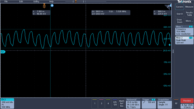
During testing, we observed that out of 10 assembled devices, 7 were not working. On these non-functional units, we measured the waveforms on the data lines of the board and observed flat (inactive) signals across all lines.

We have thoroughly inspected the soldering from all sides and did not find any issues. Additionally, we experimented with different termination resistor values (10 ohms, 22ohms, and 33ohms), but the behavior remained unchanged. we have tested the same camera module works in other device to confirm the camera is working. also we have tried diffrent values on config lines as per the table given in the schematic.

For further analysis, the relevant waveform captures and schematic images have been compiled in the attached document. The document includes:

  • Waveforms of the data lines on a non-working board
  • Waveforms of the data lines on a working board
  • Waveforms of the reset line on the non-working board

All images are included in the attached document for reference.SN65DPHY440 Retimer Not Passing MIPI Data – Flat Line Issue.docx 

Query
Can you please let us know what register settings we can try to resolve the issue or get any meaningful data by reading any registers?
  • Hi,

    1. Reset has an internal 300k pullup, so we could remove Q26 and R361 to create a passive reset circuit, remove any possible question on the power on reset timing

    2. The schematic looks ok. Can you please measure the input signal of the DPHY440? As a MIPI re-timer, DPHY440 expects to see the LP11-LP01-LP00 sequence at its input before transition to HS state. 

    3. Are you seeing issue only on lane 0 or all lanes? Lane 0 is a special lane, please see this FAQ for the detail on lane 0,  [FAQ] SN65DPHY440SS: What is the design constraint for DPHY440 lane 0 when using in a MIPI CSI design? 

    Thanks

    David 

  • Hello David,

    Thanks for your reply

    here we have attached the image of waveforms on Clock (Measured on pin no. 5 of SN65DPHY440SSRHRT).


  • Hi,

    Is this a single-end measurement and is C2 the P or the N channel? If it is, can you please measure both DACP and DACN? Can you also zoom in on the first LP to HS sequence to make sure there is a proper LP sequence?

    Thanks

    David

  • here is attached the file in which all the signals are capturedMIPI CSI_20260410.xlsx

  • Hi,

    Is Channel 1 the P and Channel 2 the N? 

    I believe this should be DACP/N measurement since it is between the camera module and the retimer. But after the LP sequence, I don't see the camera driving the HS clock signal as circled below.

    On the lane 1, what is the timing duration of the circled area and what is the data rate you are running? The circled area is the LP00 state and needs to meet the min of 40ns + 4UI and max of 85ns + 6UI to be a valid LP00.

    Thanks

    David

  • Hi David,

    The time duration in the circled area is 600nS and the current data rate on each lane is near around 62 Mbps

    (FYR: Resolution 720x576 and 30 fps and RAW 10 bit).

    Please let me know if you need any other data.

    Thanks,

    Nikhil

  • Nikhil

    If the data rate is 62MP, then this is outside of DPHY440 supported data rate. 

    The minimum supported data rate is 200Mbps and maximum supported data rate is 1.5Gbps. 

    Is there a way you can provide a higher resolution to bump up the data rate?

    Thanks

    David

  • David,

    We have already tested with a higher resolution, but the camera output on the display was highly flickering. After reducing the resolution, we were able to achieve stable video streaming from the camera.

    Additionally, I would like to highlight one more point regarding the retimer section. As per the datasheet, the I2C signals interfacing with the processor are specified for 1.8V operation. However, in our design, these signals are connected to the processor’s 3.3V pins with 3.3V pull-up resistors. Could this mismatch have any impact?

    We are raising this concern because, in some units, the camera is functioning properly, while in others, the display output is either flickering or not appearing at all.

    Thanks,
    Nikhil

  • Nikhil

    For the I2C bus, the levels of the logical ‘0’ (LOW) and ‘1’ (HIGH) are not fixed and depend on the associated level of VDD. Input reference levels are set as 30 % and 70 % of VDD; VIL is 0.3VDD and VIH is 0.7VDD. The issue is more on the VIH. Depends on whether I2C is being pulled up to 1.8V or 3.3V, if the I2C is being pulled to 1.8V, then the SoC may not detect a valid low and DPHY440 I2C register read/write may not work correctly. If the I2C pullup is 3.3V, then the DPHY440 I/O may get damaged as its absolute max rating is 2.175V.

    But DPHY440 can work without the I2C configuration, it can also work in pin strap mode. So my recommendation is to disconnect the I2C bus, and use pin-strap mode to configure the DPHY440. 

    For higher resolution flicking, have you tried to change the DPHY440 EQ, ERC, VSADJ and PRE once it is in the pin-strap mode?

    Thanks

    David

  • Hi David,

    I wanted to share an additional observation from recent measurements on the re-timer IC. While probing DA0P and DB0P, the signal at DB0P appears to be significantly attenuated or suppressed.

    Could you please advise on what might be causing this issue? I’ve included an image for your reference. In the attached image, the waveform in blue represents DA0P, and the waveform in red represents DB0P.

    Also, on some boards, although a signal is present at DA0P, there is no observable output at the DB0P pin.

    Note:

    • DA0P is directly connected to the camera module.
    • DB0P is directly connected to the processor.

    Please let me know your thoughts.

    Best regards,

    Nikhil

  • Nikhil

    For the measurement at DB0P, are you measuring at the far end? If you are measuring at the far end, then the signal could be attenuated by the PCB trace or cable insertion loss. The DPHY440 TX provides 0dB or 2.5dB pre-emphasis which can help compensating some of the PCB trace/cable insertion loss. 

    For not seeing the signal at DB0P, the DPHY440 lane 0 is a special lane as it is also being used as a backchannel lane for DSI. For detail on lane 0, please take a look at this E2E FAQ and the requirement on lane 0 for CSI,  [FAQ] SN65DPHY440SS: What is the design constraint for DPHY440 lane 0 when using in a MIPI CSI design? 

    Any chance you can share your layout for review as well?

    Thanks

    David 

  • David

    I have measured the waveform on the exact pin of the IC only not on any other end.

    Here i attached the images of layout with length of nets, let me know if you need any other data.

  • Hi,

    The DPHY440 looks to be placed closer to the camera than the processor. In this case, then you are not taking advantage of DPHY440 receiver EQ and De-skew capability. 

    Looking at the routing on the input side, there are via as signals get routed between different layer. Do you have GND stitching via next to the signal via for the current return path? 

    For the measured waveform, are these measured with high impedance active probe?

    Thanks

    David 

  • Hi,

    1. The re-timer is currently placed closer to the camera than to the processor.
    2. We have added GND stitching vias adjacent to the signal vias to maintain a proper return path.
    3. For waveform measurements, I used probes with the following specifications: 3.9 pF input capacitance, 10 MΩ impedance, 300 V CAT II rating, and 500 MHz bandwidth.

    Additionally, I would like to highlight two important points:

    1. We cannot ignore the LP state, as camera sensor is asserting LP state.
    2. To enter the LP state, we attempted to exit shutdown mode by toggling the RESET line (low-to-high transition, as per datasheet page 13), allowing the Retimer to switch into LP mode. This was tested on three boards, and as a result, video output started but appeared flickered. Previously, the system was getting stuck at the LP-11 state with a wait timeout.

    Is there any other config apart from disabling LP mode to handle this kind of scenario?

    please suggest any further steps or possible solutions to stabilize the stream and eliminate the flickering.

  • Hi,

    I would not use DPHY440 reset to switch into LP mode if possible. Once the payload data transmission has been completed, the camera needs to toggle the differential state immediately after last payload data bit and keeps that state for a time THS-TRAIL(Refer to Table 14 of the MIPI spec). The camera will then disable the HS-TX, enables the LP-TX, and drives Stop state (LP-11) for a time THS-EXIT(min 100ns). 

    With DPHY440 lane 0 being a bi-directional lane, the processor also needs to make sure it provides the proper LP entry/exit sequence so the DPHY440 can properly enter/exit the LP.

    On the camera side, is it possible to disable LP and enable HS only? We do have I2C registers that can disable LP and enable HS only in DPHY440 as well. If this is possible, then I want to see if it eliminates the flickering issue you are seeing.

    Thanks

    David