DP83869HM: Request for Schematic Pre-Check and Ethernet PHY Design Validation – AM2634 + DP83869

Part Number: DP83869HM
Other Parts Discussed in Thread: DP83869, AM2634

Hello TI Team,

I have designed a custom industrial board based on the AM2634COLFHAZCZR (Sitara™ Real-Time MCU) along with the DP83869 Gigabit Ethernet PHY.

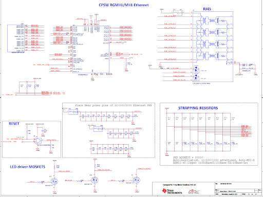
Before proceeding with Ethernet bring-up, PHY initialization, and continuous ping stability testing, I would like to request a detailed schematic pre-check and design validation from the TI team to ensure the hardware implementation follows TI recommended guidelines and reference designs.

Our intention is to validate the schematic thoroughly before PCB fabrication/board bring-up to avoid any Ethernet stability.

Processor : AM2634COLFHAZCZR (Sitara™ Real-Time MCU)

Ethernet PHY:  DP83869 Gigabit Ethernet PHY

Ethernet Interface:  RGMII interface between AM2634 and DP83869

Target Validation:

  • Ethernet PHY bring-up
  • MDIO communication verification
  • PHY link detection
  • Continuous ping stability testing
  • Long-duration Ethernet communication validation

    Please review the RGMII interface between AM2634 and DP83869.

    Signals include:

    • TXD[3:0]
    • RXD[3:0]
    • TX_CTL / RX_CTL
    • TX_CLK / RX_CLK
    • MDC / MDIO

    Please verify:

    • Signal connectivity correctness
    • IO voltage compatibility
    • Pull-up/pull-down requirements
    • Trace matching recommendations
    • RGMII timing/skew implementation

    Specific Questions:

    • Should DP83869 be configured with internal delay mode or external PCB delay?
    • Are series termination resistors recommended on RGMII signals?
    • Are there any layout-critical timing considerations?
      1. Clock Network Verification

      Please review:

      • 25MHz crystal circuit connected to DP83869
      • Crystal load capacitor values
      • Clock routing recommendations
      • Oscillator stability requirements

      Questions:

      • Is the crystal implementation correct as per TI recommendations?
      • Are the load capacitor values appropriate?
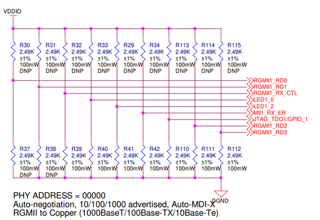
        1. PHY Strap Pin Configuration

        Please verify:

        • PHY address strap configuration
        • RGMII mode strap settings
        • Bootstrap resistor values
        • Auto-negotiation configuration
        • LED strap functionality

        Questions:

        • Is the PHY correctly configured for RGMII operation?
        • Is Auto-negotiation enabled correctly by default?
        • Any strap timing or resistor concerns?
          1. Reset Circuit Verification

          Please review:

          • Reset topology for AM2634 and DP83869
          • Reset timing implementation
          • Reset dependency between MCU and PHY
          • Power-on reset behavior

          Questions:

          • Is the reset timing correct?
          • Is the reset sequence proper for reliable PHY initialization?

            Request

            Kindly review the attached schematic and provide feedback on whether the design is ready for PCB fabrication and hardware bring-up.

            Please let us know if:

            • Any schematic corrections are required
            • Any layout recommendations should be followed
            • Any Ethernet timing or PHY configuration changes are needed before fabrication
              CUSTOM_BRD_REV03.pdf 


  • Hi Phanendra,

    I can help review your implementation of the DP83869. Have you already reviewed the schematic checklist for the device, as well as the layout checklist

    Best regards,

    Greg

  • Hi Gregory,

    Thank you for valuable response
    We are under checking schemtic with reference to your attched schematic checklist . once layout and schematic we will let you 

    Thank you .

  • Hi Phanendra,

    Sounds good, thank you.

    Best regards,

    Greg

  • Dear Gregory,

    Please find the attached Excel sheet containing the layout and schematic review checklist.

    Kindly review the PHY-related design and the RGMII section, and let us know if you have any observations or recommendations.Copy of DP83869_Schematic_Checklist_RevC (public)_Updated.xlsxSNLR048A_Open list from Customer-UPDATED.xlsx

    Best regards,
    Phanendra

  • Hi Phanendra,

    Thank you for sharing the checklists. I will review the documentation and provide comments next week.

    Best regards,

    Greg

  • Dear Gregory,
    Thank for your response . we are eagerly waiting for your confirmation

  • Hi Phanendra,

    I will provide the comments, thank you!

    Best regards,

    Greg

  • Hi Gregory

    Could you please review our project Gerber files and PCB layout PDF attached.

    We would appreciate your feedback and confirmation before we proceed with PCB fabrication. If you have any observations or recommendations, please let us know so that we can incorporate them before releasing the design for manufacturing.

    Thank you for being so supportive.
    BLIS-CUST-_BLIS_CUSTOM_BOARD_REV03-29062026-172.pdf

    Best regards,

  • HI Phanendra,

    I can help review the layout. Is it possible to share the actual layout file (.brd or similar)? That way I can more accurately review trace routing and other aspects.

    Best regards,

    Greg

  • Hi Gregory,
    Please find attachement of board file which  we have did in allegro . please kindly review and provide your feed back asap

    Thank you
    Phanendra kumarBLIS_CUSTOM_BOARD_REV03-29062026-172 (2).zip

  • Hi Phanendra,

    Thank you, I will provide feedback as soon as possible.

    Best regards,

    Greg

  • Hi Gregory
    Please kindly provide your feedback. We are waiting to release to PCB manufacturing
    Thank you

    Phanendra kumar

  • Hi Gregory
    This is gentle remiander we are eagerly waiting for your comments . we need to release to PCB manufaturing please kindly respond on this 
    Thank You

    Phanendra Beella

  • Hi Phanendra,

    Here are some of my comments on the design:

    • If a 1.2V supply is used for the VDD1P1 pin, it is advised to be careful, as the datasheet listed 10% tolerance is usually for supply ripple.
    • As I did not see a resistor description, I wanted to confirm the correct resistance on the MDI was used 
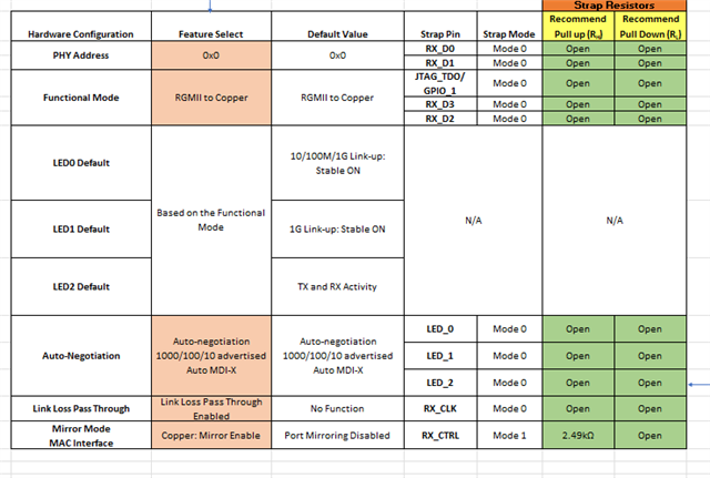
    • Please make sure the strap tool in the schematic checklist is used to configure the straps to the intended modes, I was not sure if the current strap resistors are the intended ones for the design
    • The traces should be length matched within 20 mils for 1G transmissions and within 50 mils for 100M or 10M transmissions.
    • For components like transformer/magnetics, chokes, AC coupling capacitors and ESD diodes, a two-layer void is recommended for Standard applications
    • Please follow all points in the Ethernet PHY PCB Design Layout Checklist

    Best regards,

    Greg

  • Hi Gregory,

    Thank you for your review and valuable comments. Please find our responses below.

    1. VDD1P1 Supply (1.2 V)
      • We have already updated the VDD1P1 power net to 1.1 V as recommended.
    2. MDI Resistor Values
      • We have used the same resistor values as those used in the TI EVM design.
    3. Strap Resistor Configuration
      • We have followed the same strap resistor values and configuration as the TI EVM design.
    4. Trace Length Matching
      • We have already verified the PCB through simulation. All Ethernet signals meet the required constraints, and as shared earlier, we have followed the recommended PCB design checklist during the layout.
    5. Magnetics, Chokes, AC Coupling Capacitors, and ESD Diodes
      • We have used the same components as the TI EVM design. The only exception is the RJ45 connector, for which we selected an equivalent alternative part with matching specifications.
    6. Ethernet PHY PCB Design Layout Checklist
      • We will review all the items in the Ethernet PHY PCB Design Layout Checklist once again and implement any additional recommendations if required.

    Could you please review the PCB layout and share your feedback? If everything looks good from your side, kindly let us know so that we can proceed with the next steps.

    Thank you for your support.

  • Hi Phanendra,

    MDI Resistor Values
    • We have used the same resistor values as those used in the TI EVM design.

    Here, I was referring to the populated resistors on the strap:

    The strap tool in the schematic checklist should be used to select the correct straps according to the desired PHY features

    Best regards,

    Greg

  • Hi Gregory,

    Thank you for your reply.

    We are following the same strap resistor configuration as the TI EVM board. For your reference, I have attached a screenshot of EVM  schematic showing the strap resistor configuration.

    Our design uses an RGMII-to-Copper interface, similar to the TI EVM. Could you please confirm whether there are any differences in the required strap resistor configuration between a custom board and the TI EVM for this interface?

    Please let us know if you recommend any changes to our current configuration.

    Thank you for your support.

    Best regards,
    Phanendra

  • Hi Phanendra,

    Is this the same schematic as the EVM schematic listed in on the EVM web page?

    https://www.ti.com/lit/df/snlr042/snlr042.pdf

    Here there are options to populate the headers for the strap pins. 

    As shown in the strap tool checklist, GPIO_1, RX_D3, and RX_D2 should all be OPEN for RGMII to copper mode.

    Best regards.

    Greg

  • Hi Gregory,

    Thank you for your reply

    We will follow same stap tool checklist . please share your comments on layout file 
    Thank you.

  • Hi Phanendra,

    Beyond my initial comments, I did not see any problems with the layout.

    Best regards,

    Greg

  • Hi Gregory,

    Thank you for your confirmation.  We will get back while testing

    Thank you 
    Phanendra Beella

  • Hi Phanendra,

    Sounds good, thank you.

    Best regards,

    Greg

  • Hi Gregory,

    Hope you are doing well.

    We have started testing the board. The Ethernet link is coming up successfully, and the MAC loopback test is also passing.

    However, when we try the PHY loopback test, the test is failing. We are getting the following log:

    =============================
     Enet Loopback: Iteration 1
    =============================
    CPSW_3G Test
    EnetAppUtils_reduceCoreMacAllocation: Reduced Mac Address Allocation for CoreId:0 From 4 To 2
    Open MAC port 1
    EnetPhy_bindDriver:1873
    PHY 0 is alive
    initQs() txFreePktInfoQ initialized with 16 pkts
    EnetPhy_getLinkCfg:628
    Cpsw_handleLinkUp:1623
    Cpsw_periodicTick:731

    From the above log:

    • MAC port 1 is opening successfully.
    • PHY 0 is detected and alive.
    • Link-up is successful.
    • PHY loopback is failing.

    Could you please review the above log and guide us on what we should check or modify to get the PHY loopback test passing?

    We are using the AM263x platform with the TI Enet/LwIP example.

    Please suggest the next debug steps or any specific PHY loopback test passing.

    Thank you 
    Phanendra Beella

  • Hi Phanendra,

    I will look into this an get back to you as soon as possible.

    Best regards,

    Greg

  • Hi Gregory,

    After adding a few comments in the code, we are now able to see the TX packet transmission log. However, we are still not receiving any RX packets, and the RX interrupt is not being triggered.

    Please find the latest loopback log below:

    =============================
     Enet Loopback: Iteration 1
    =============================
    CPSW_3G Test
    1
    2
    3
    EnetAppUtils_reduceCoreMacAllocation: Reduced Mac Address Allocation for CoreId:0 From 4 To 2
    Open MAC port 1
    EnetPhy_bindDriver:1873
    PHY 0 is alive
    4
    5
    6
    initQs() txFreePktInfoQ initialized with 16 pkts
    7
    8
    10
    11
    MAC PORT = 1
    12
    13: status=0 linked=0
    GET_LINK_CFG: status=0 speed=1 duplex=0
    Cpsw_handleLinkUp:1653
    12
    13: status=0 linked=1
    GET_LINK_CFG: status=0 speed=1 duplex=1
    9
    BEFORE TX DONE WAIT
    Transmitted 5000 packets
    Delete EnetApp_txTask() and exit..
    TX DONE RECEIVED
    BEFORE RX DONE WAIT

    From the above log, our current observation is:

    • TX packets: 5000 packets are being transmitted successfully.
    • TX completion: TX DONE is received.
    • RX packets: No RX packets are received.
    • RX interrupt: RX interrupt is not being triggered.
    • PHY: PHY 0 is detected and reported as alive.
    • Link: Link is reported as up with 1 Gbps, full duplex.

    Could you please check and advise whether any hardware changes or software/code changes are required to get the RX packets?

    In particular, could you please guide us on what we should check next in the following areas:

    1. CPSW MAC RX path
    2. RX DMA/RX descriptor configuration
    3. RX interrupt configuration and interrupt enable
    4. RGMII RX signals between the PHY and AM263x
    5. DP83869 PHY loopback configuration
    6. PHY strap/configuration settings related to RGMII
    7. Any specific registers or software debug points that we should check to determine where the RX path is stopping

    Also, during the ping test, we captured the following DP83869 register values:

    ============= DP83869 FULL DUMP =============
    
    Reg[0x00] (BMCR)        = 0x1140
    Reg[0x01] (BMSR)        = 0x796D
    Reg[0x02] (PHYIDR1)     = 0x2000
    Reg[0x03] (PHYIDR2)     = 0xA0F3 ------- A0F1
    Reg[0x04] (ANAR)        = 0x01E1
    Reg[0x05] (ANLPAR)      = 0xCC01
    Reg[0x06] (ANER)        = 0x006F
    Reg[0x07] (ANNPTR)      = 0x2001
    Reg[0x08] (ANNLPTR)     = 0x4006
    Reg[0x09] (GEN_CFG1)    = 0x0200
    Reg[0x0A] (GEN_STATUS1) = 0x7800
    Reg[0x0B] (RESB)        = 0x0000
    Reg[0x0C] (RESC)        = 0x0000
    Reg[0x0D] (REGCR)       = 0x0000
    Reg[0x0E] (ADDAR)       = 0x0000
    Reg[0x0F] (1KSCR)       = 0xF000
    Reg[0x10] (PHY_CONTROL) = 0x5048
    Reg[0x11] (PHY_STATUS)  = 0xBF02
    Reg[0x12] (INT_MASK)    = 0x0000
    Reg[0x13] (INT_STATUS)  = 0x1C42
    Reg[0x14] (GEN_CFG2)    = 0x29C7
    Reg[0x15] (RX_ERR_CNT)  = 0x0000
    Reg[0x16] (BIST_CONTROL)= 0x0000
    
    ------ C22 EXTENDED REGISTERS ------
    
    Reg[0x17] (STATUS2)     = 0x0040
    Reg[0x18] (LEDS_CFG1)   = 0x6150
    Reg[0x19] (LEDS_CFG2)   = 0x4444
    Reg[0x1A] (LEDS_CFG3)   = 0x0002
    Reg[0x1E] (GEN_CFG4)    = 0x0012
    Reg[0x1F] (GEN_CTRL)    = 0x0000

    Please review the above log and register dump and let us know if there are any specific changes or additional checks required on the hardware or software side.

    Thank you 
    Phanendra Beella

  • Hi Gregory,

    We have been waiting for your response since last week.

    We have now made some progress with the board. The PHY loopback test is working successfully, and we are also able to perform the ping test. However, the ping test is not stable when running for a longer duration.

    We are currently observing a strange behavior where the code appears to be getting erased from the MCU by itself during/after the test.

    Could you please help us understand what could cause this type of behavior?

    We can share the test code, console logs, register values, and waveforms if required.

    Please suggest what checks we should perform to identify why the MCU code is getting erased.

    Thank you 
    Phanendra Beella

  • Hi Phanendra,

    Gregory is out of office so I will be stepping in to help. Glad to hear the loopback test is working, but for my own understanding, is 'PHY loopback' referring to MII loopback or to reverse loopback? Basically, what register value are you setting when performing PHY loopback?

    We are currently observing a strange behavior where the code appears to be getting erased from the MCU by itself during/after the test.

    Is this saying the MCU is not saving data while you are performing ping? If so, this may be a better question for the AM263x team as Gregory and I only support our ethernet PHYs. Have you reached out to this team on E2E already, or if not I can loop them in on this thread.

    Best,

    Shane